
It has been a week since my last post and I am sorry for that! I am currently moving to my new place in Houston where I work for Dynamic Perception. The Dual motor controller booster pack will arrive next Monday.
IEE Flip VFD Driver Code
IEE Flip VFD Working! Test code coming soon.
Today I wrote some code to get the IEE Flip VFD working. It has a fairly simple protocol and only took a bit of tweaking to get it working. I wrote the demo code for my Prop Dev Stick and will be uploading the SPIN code later once I finish the feature set.
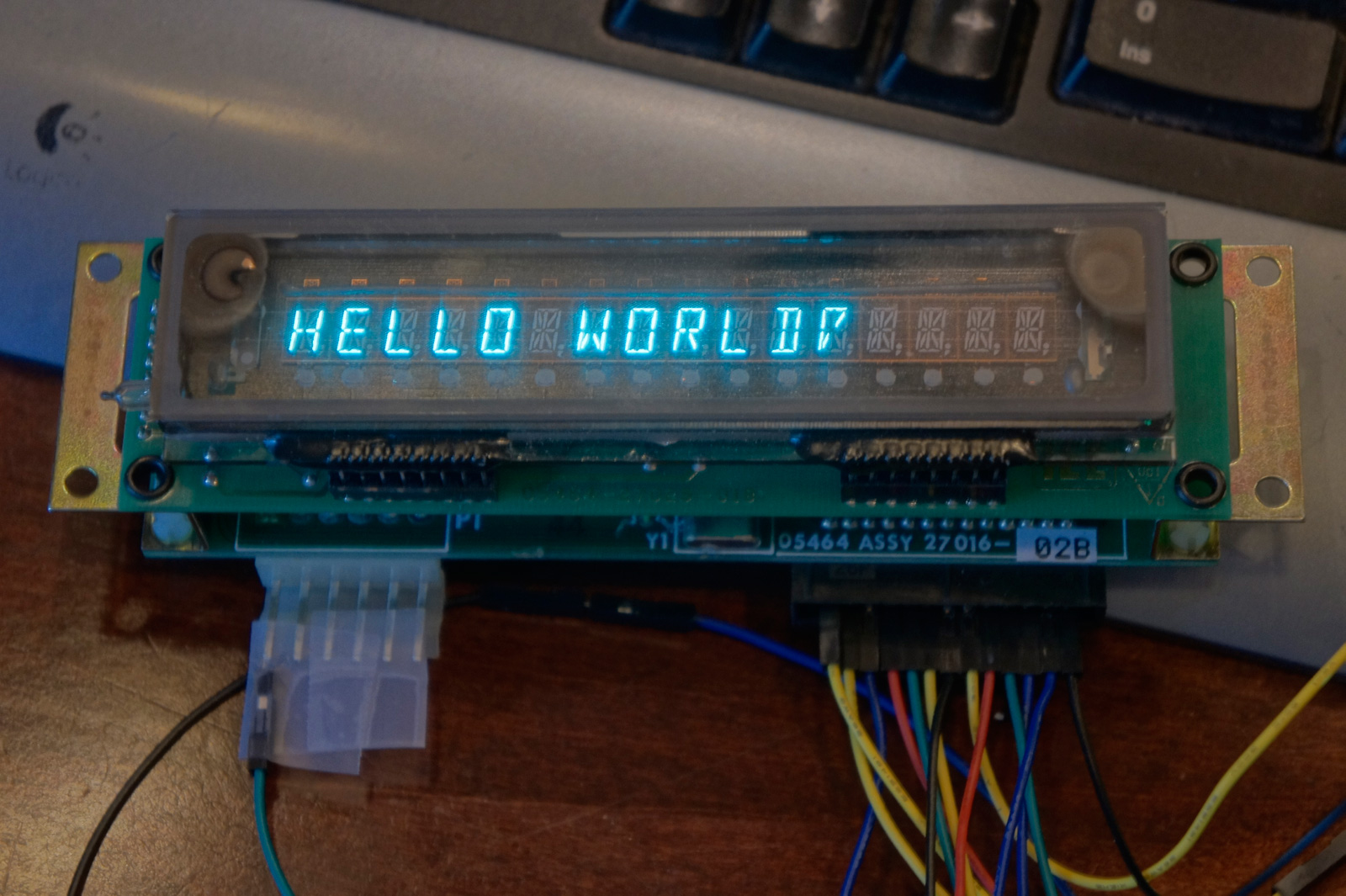
After this I will write some C code for the MSP430 LaunchPad and get that working. The screen supports a serial input mode which saves 8 I/O pins but requires more timing. I will try to get that working as well.
2A Low Voltage Motor Driver BoosterPack Ver1.2 Final?
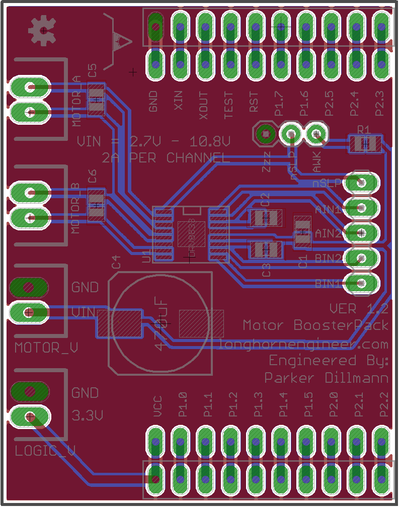
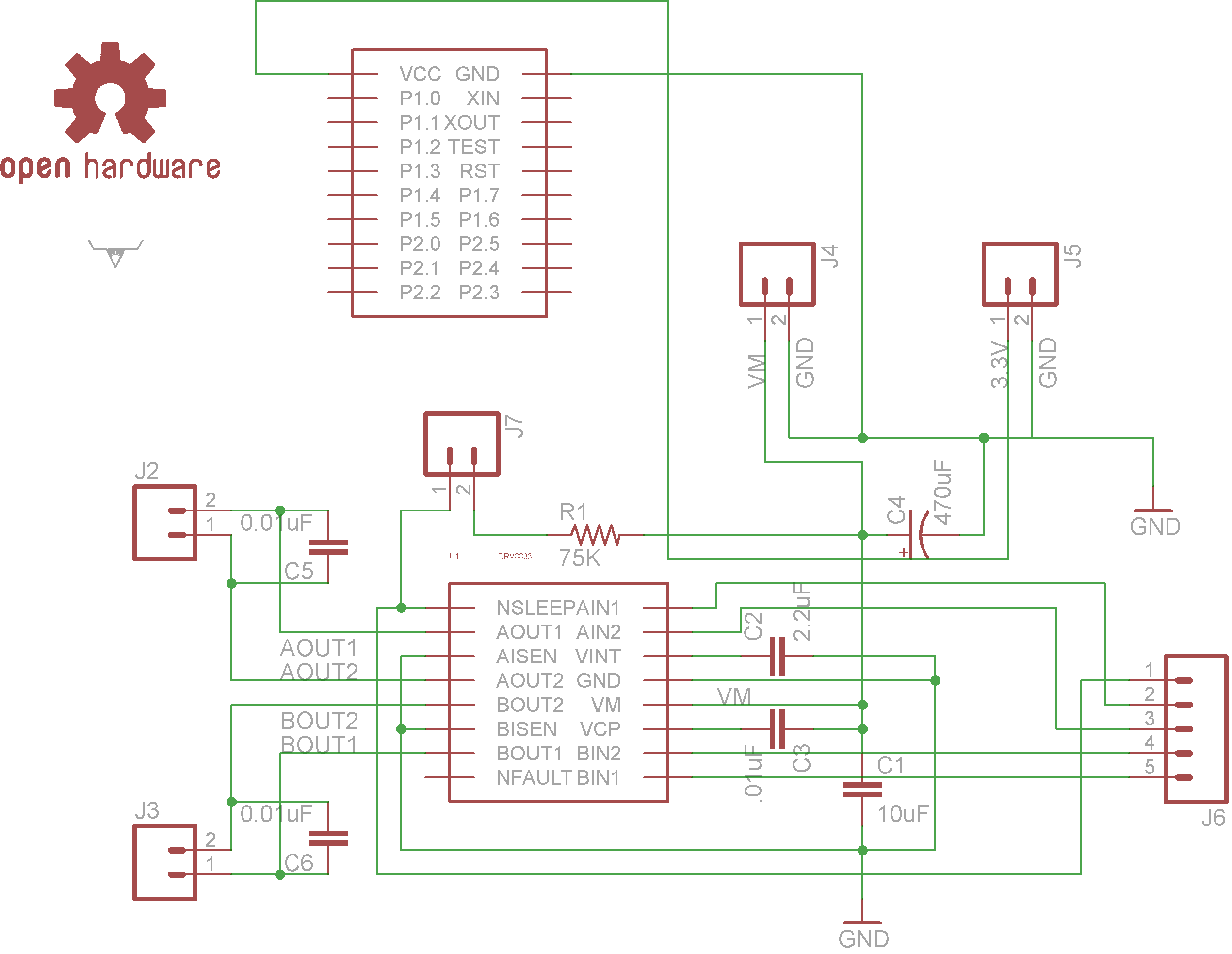
I finally think I have a version of the motor driver that I like. I tweaked the traces around the 470uF cap to make the ground path better. I also changed the nSleep jumper header from a 2-pin to a 3-pin. The user can hard wire the nSleep high or low.
2A Low Voltage Motor Driver BoosterPack Ver1.1 Released!
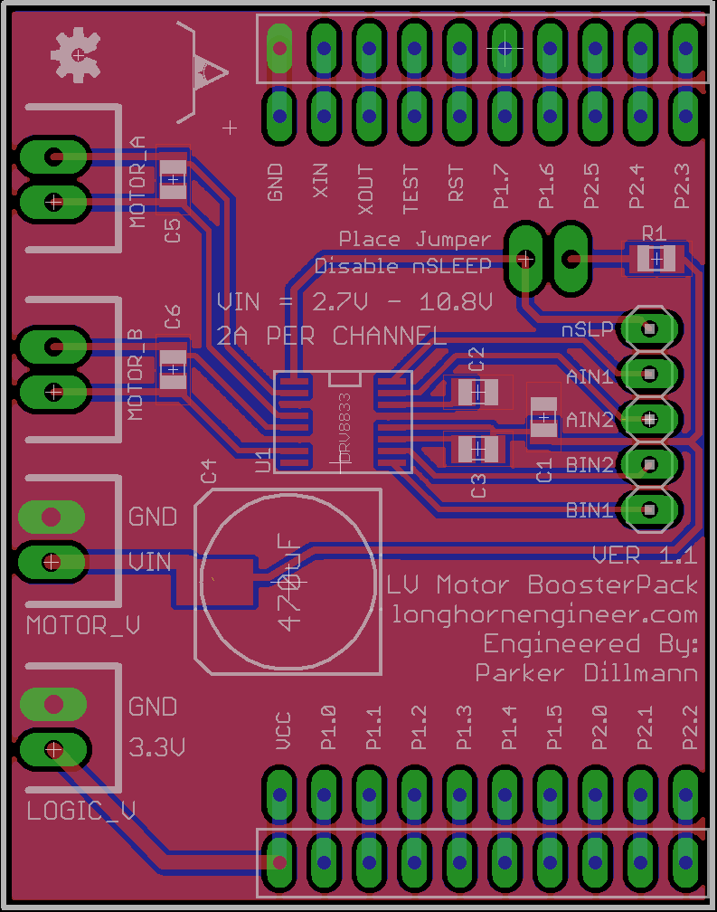
I finished up the PCB for the Motor Controller Booster pack. The PCB is all open source and you can download the files here.
Files (Eagle V6)
2A Low Voltage Motor Driver BoosterPack Ver1.0
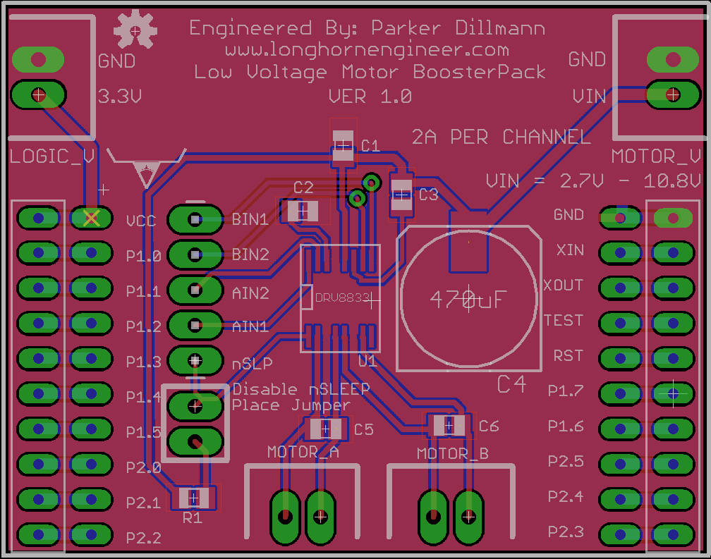
This is a Low Voltage, 2A motor controller BoosterPack for the Ti LaunchPad. So far I have not found a motor controller yet so I decided to make one. This is the first in many BoosterPacks I will be designing and selling. It uses the Ti DRV8833PWPR Dual H-bridge Motor Driver chip. The chip is capable of 2Amps per motor channel and a motor voltage from 2.7V to 10.8V. Logic voltage for the DRV8833 is 3.3V which makes it a perfect match for the MSP-430 LaunchPad.
The BoosterPack has the nSleep pin broken out from the DRV8833. Using this pin will put the DRV8833 to sleep to minimize current draw. If this pin is not needed or the LaunchPad is lacking I/O there is a jumper to pull the nSleep pin high.
Single Cell Lithium Battery Charger Circuit Ver 1.2 Released!
This circuit is designed around the MCP73837 chip. There are a couple different versions of this chip which allows the same PCB have a charge cut off voltage of 4.2V for normal lithium batteries and 4.35V for high capacity lithium batteries.
4.20V – MCP73837-NVI/UN
4.35V – MCP73837-FCI/UN
It charges via USB at a rate of 500mA or an external power supply rated at 5-6V at 1A. I would use a power supply at a rating of at least 1.2A for this charger.
Added a micro usb plug to compliment the mini usb plug and DC power jack. Made all the passive parts 0805 size to make the board easier to assemble. Tweaked the mounting holes a bit as well.
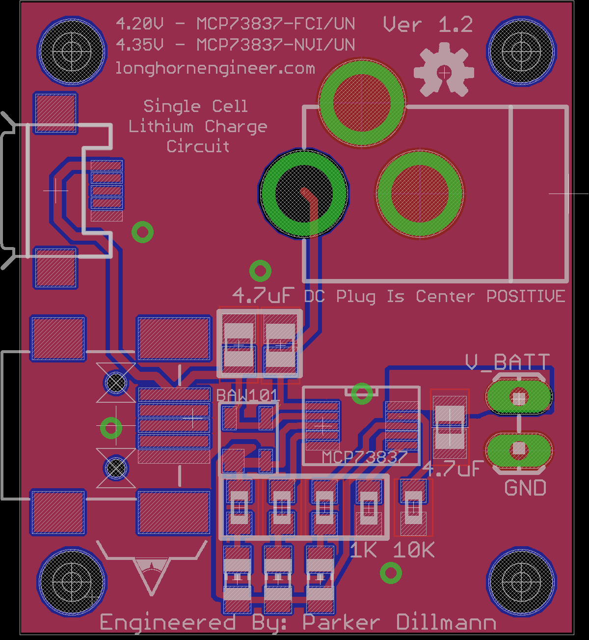
Files (Eagle V6)
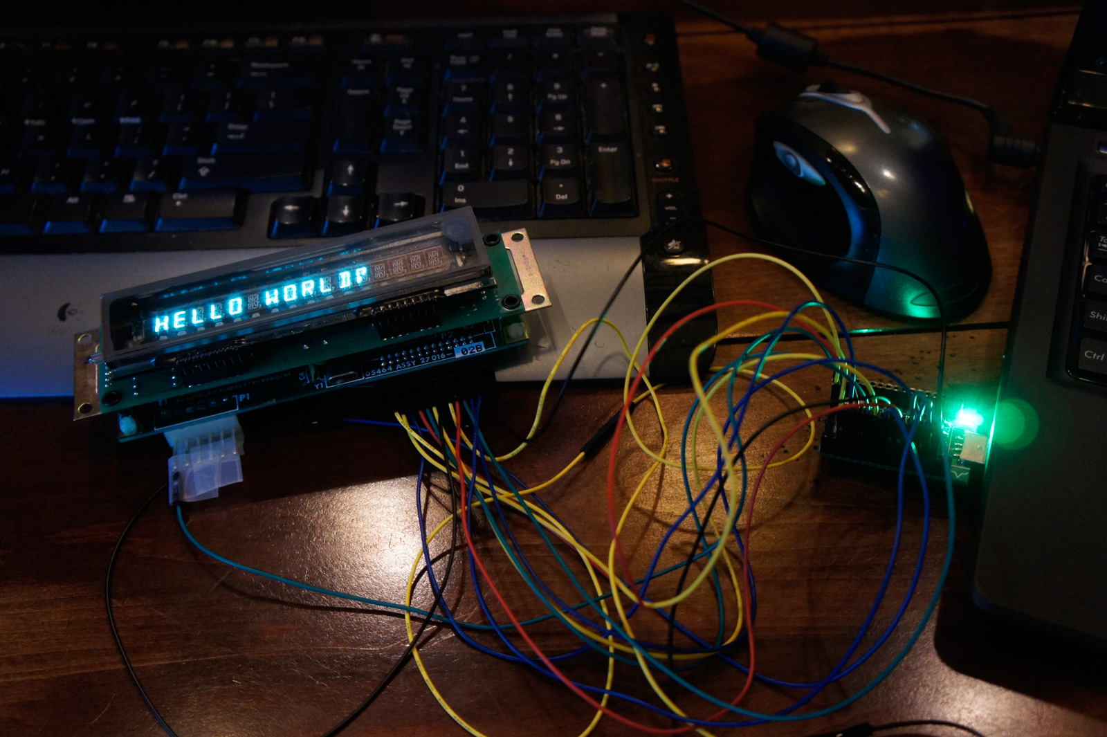
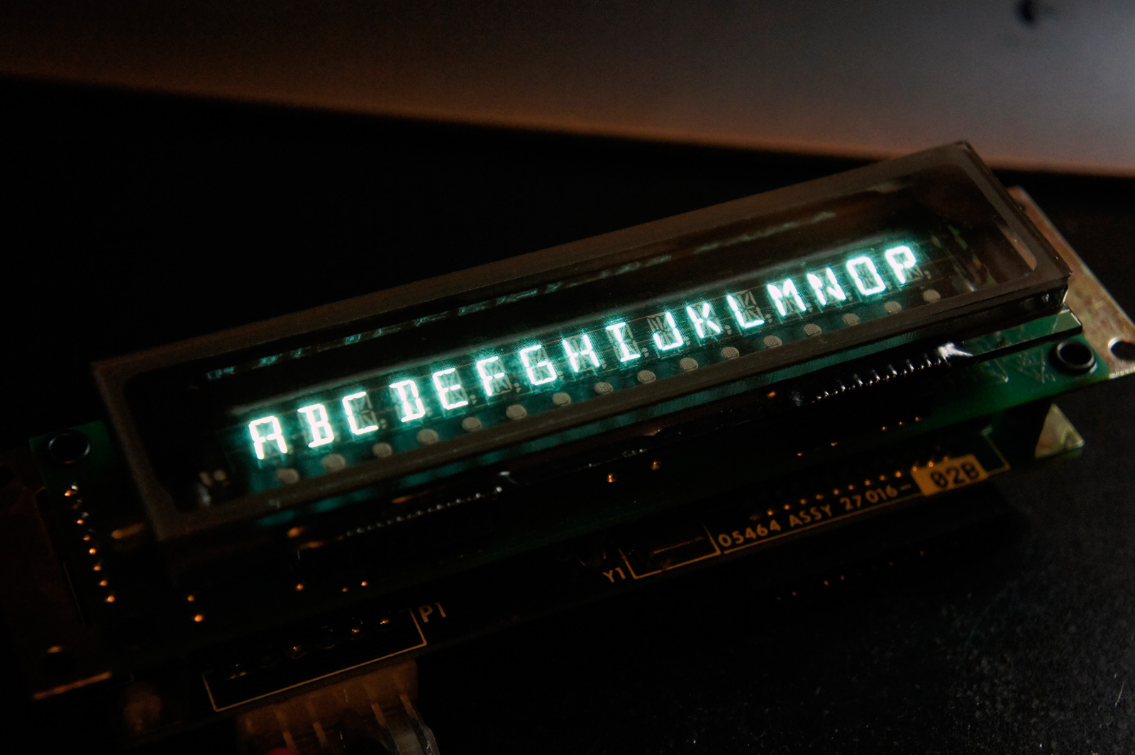
IEE FLIP Alphanumeric Display Works!
I picked up some of these really neat VFD alphanumeric displays at a surplus shop while at Maker Faire. After acquiring the datasheet from the manufacture, I decided to test them with the built in test mode. I have already started writing the code to run the display and will be posting the code and datasheet when it is done.
Super Boost running off of AA batteries. Just because it can.

Super Boost charging my phone off of two AA batteries.
I think that is enough update posts for right now.
NES 2 (Top Loader) Portable now ready for Maker Faire
Here is a status update for the NES Top Loader portable!
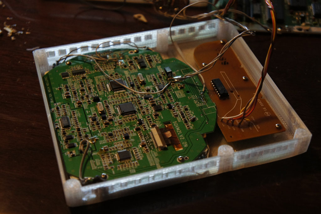
Assembling the front half of the case. Using size M2 sheet metal screws to attach the PCBs to the case. Holes are tapped with a 1.5mm drill bit before hand. For those that know the PSone screen accepts 7.4V then converts it down to 5V in some areas with a 7805 linear regulator. I removed the 7805s and attached my 5V switching power supply to the pads which dropped the power draw of the screen.
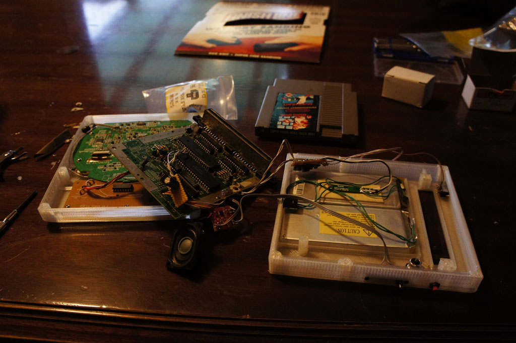
The back side houses much more parts. Batteries, switching powersupply, NES Top Loader PCB, speaker, amplifier, and volume control are all housed here. There is no hotglue in this portable. Everything is mechanically held in place. Some electrical tape is used to insulate parts but that is about it.
Continue reading NES 2 (Top Loader) Portable now ready for Maker Faire