I decided to go with the ICD15S13E4GX00LF VGA connector. Was slightly less expensive and had a better mechanical drawing to convert to a footprint.
I decided to go with the ICD15S13E4GX00LF VGA connector. Was slightly less expensive and had a better mechanical drawing to convert to a footprint.
This is something I recorded with Stephen Kraig (Co-host of the MacroFab Engineering Podcast) back in September 2016. We never made it public till now! Drunken Gaming Night! It is silly and I have no idea where Stephen and I will take the channel but it is fun to do.
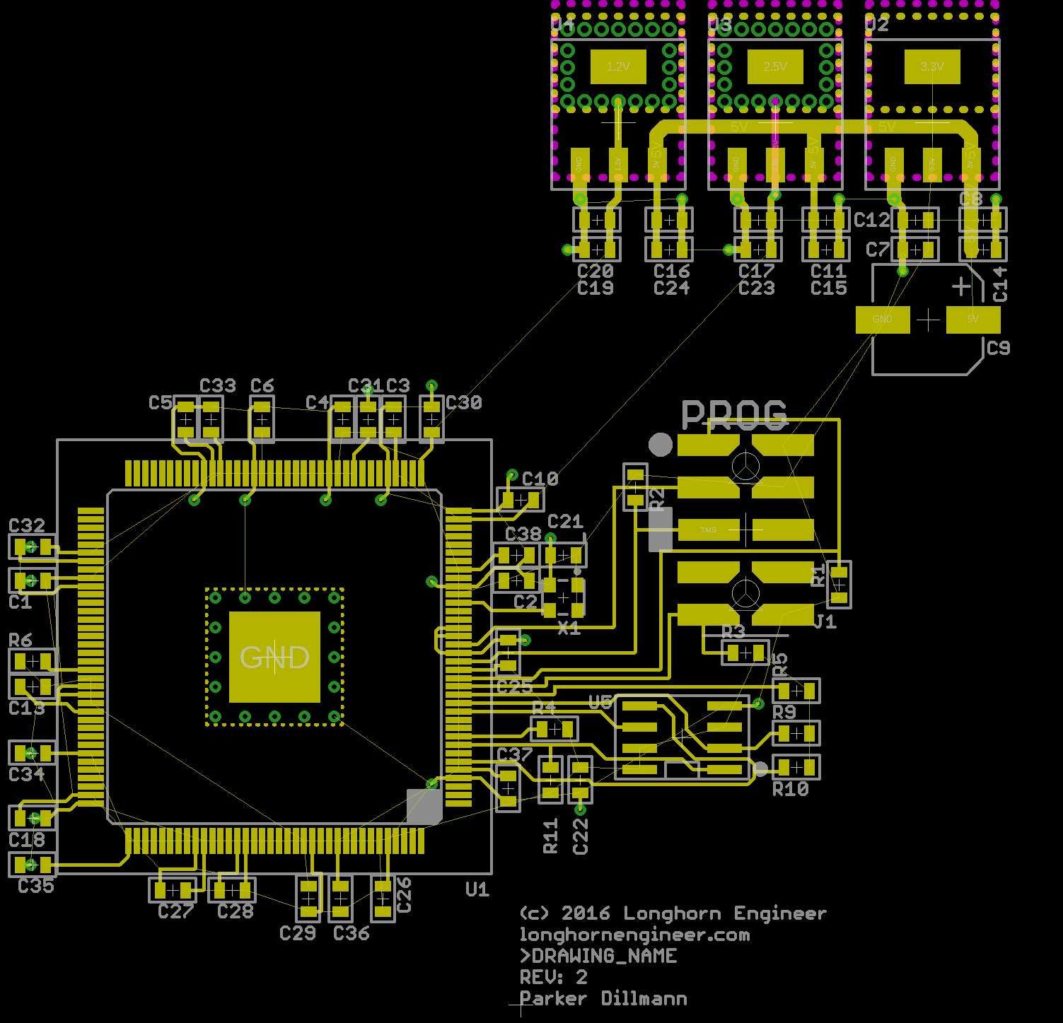
Things to finish on the Gameboy VGA Design
The DMG-01 Gameboy runs off all 5V logic and the FPGA I will be using (Cyclone 4 Altera) runs off 3.3V I/O. Conversion is needed to prevent frying the FPGA. I have used the TI part SN74LVC8T245 in the past with other FPGA projects and on the proof of concept VGA mod with the DE0 dev board.
The SN74LVC8T245’s output enable is active low so I pulled it high with a 10K resistor. This way the convertor is disabled till the FPGA can control the IC. Direction is set by default to be 5V -> 3.3V conversion with a 10K pull down.
I am also going to pull in the state of the buttons on the Gameboy. I hope to be able to have different modes that the FPGA can perform. Resolution changes and the like. Eventually I will design it so that FPGA can also drive the screen but that will probably be a future hardware revision.
Instead of trying to have an excuse of why I have not been posting here. Well go check out MacroFab. It is the company I co-founded a bit over 4 years ago now. I also am the co-host of the MEP or MacroFab Engineering Podcast. It is a weekly electronics podcast and we are currently on episode 119…and we have not missed a single week!
I have been doing side projects for fun but I have just been very bad about posting them here. Typically they just go to my twitter account and I talk about them on the podcast. I will be putting more effort into posting here.
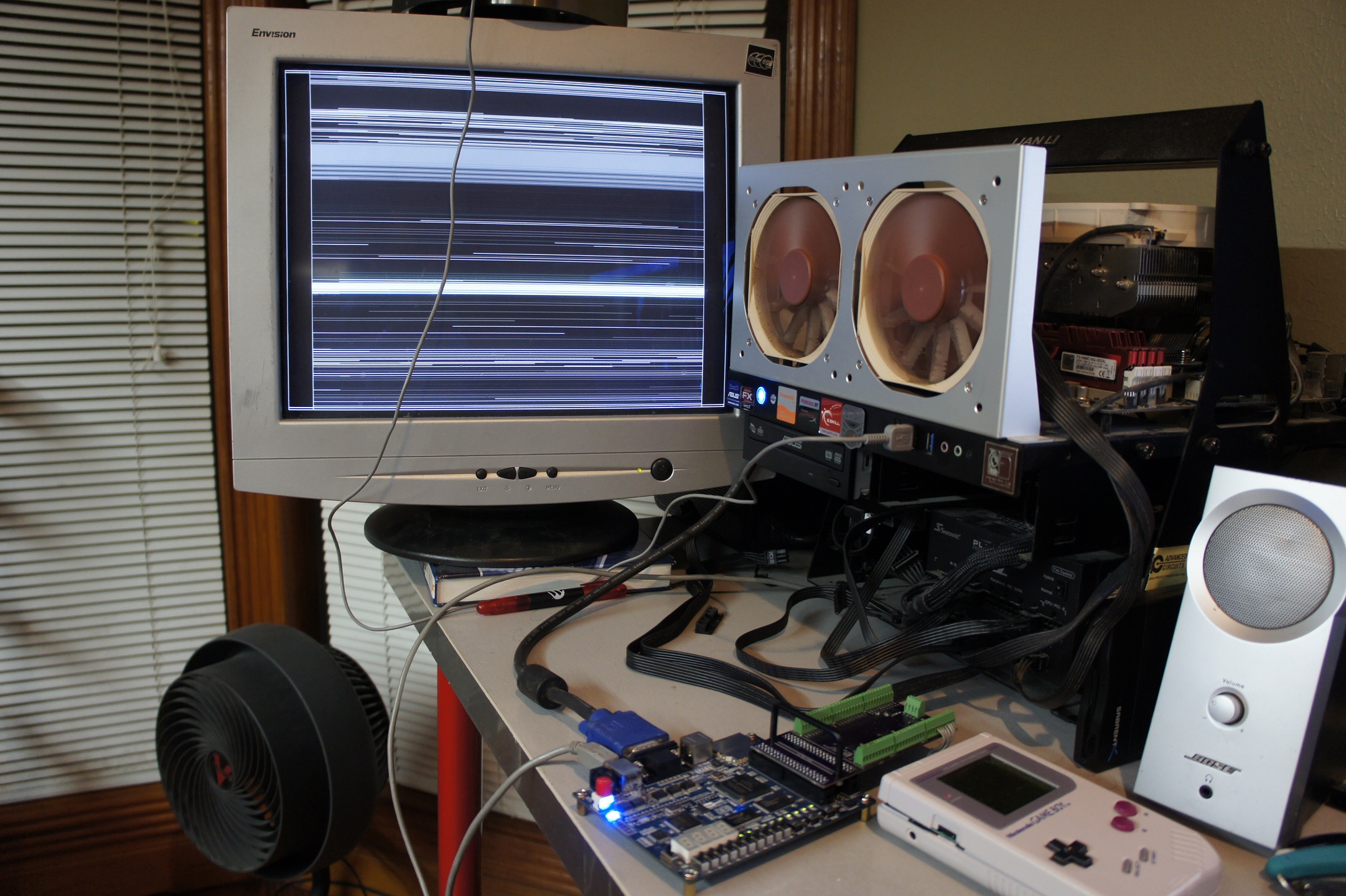
With that out of the way… Current plan is to just look at my past incomplete projects and either finish them or kill them off. Starting with the FPGA Gameboy project. First order of business is to start making some dedicated hardware for the Gameboy. To quicken the development process I am going to lift the FPGA design block from the ChromaColor project. The FPGA is an older Cyclone 4 module (EP4CE6E22C8N) but it should do the trick and is still fairly affordable. I would like to move it to a newer platform like a 10M08SCU169C8G.

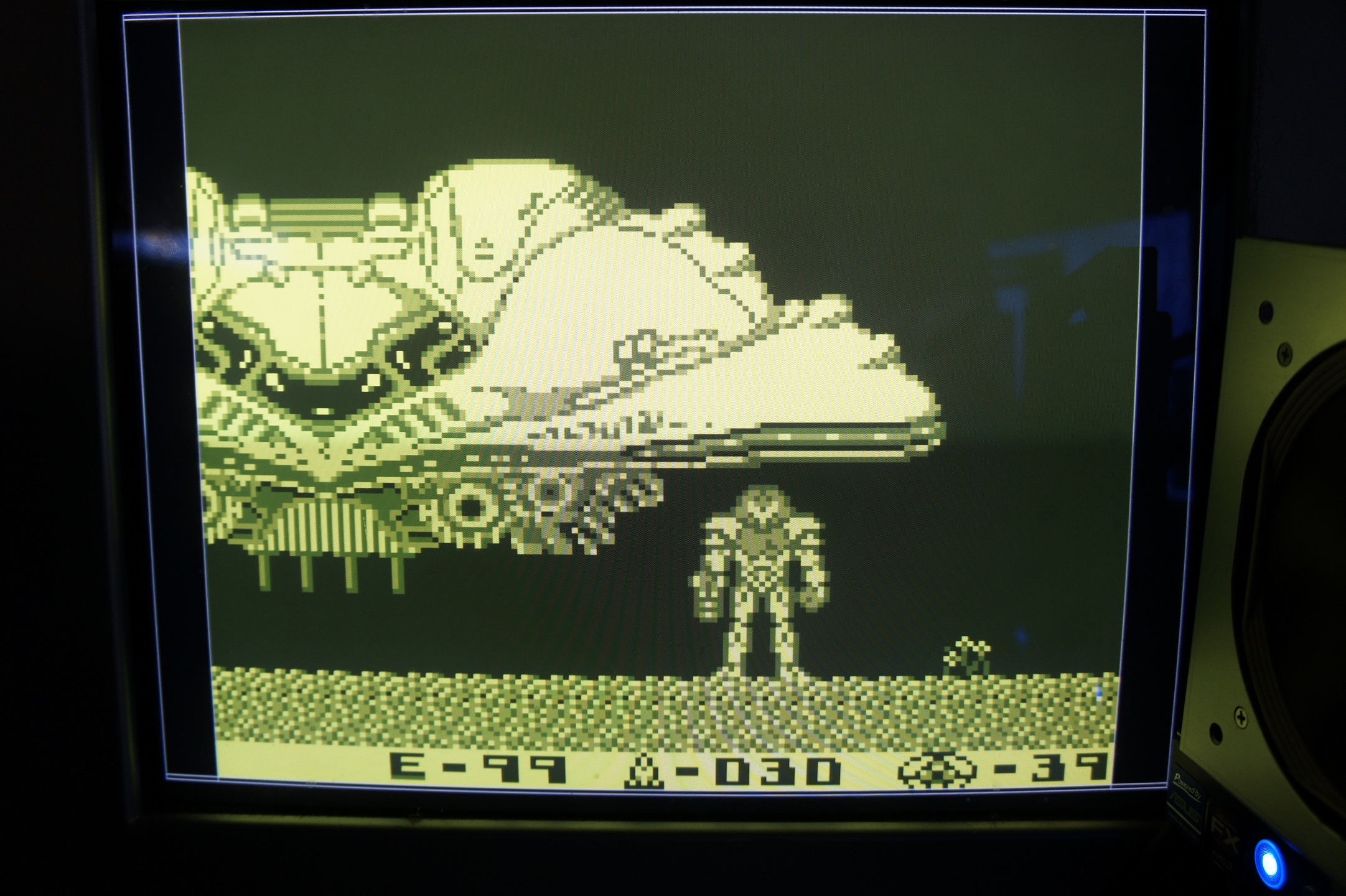
I have some seemingly random video glitches to iron out but it is much better then previously. I will probably need to recode my capture routine as a state engine to make further advancements.
Have some screen tearing and the capture code is a mess but its progress!
Edit//: More work. Fixed inverted colors.
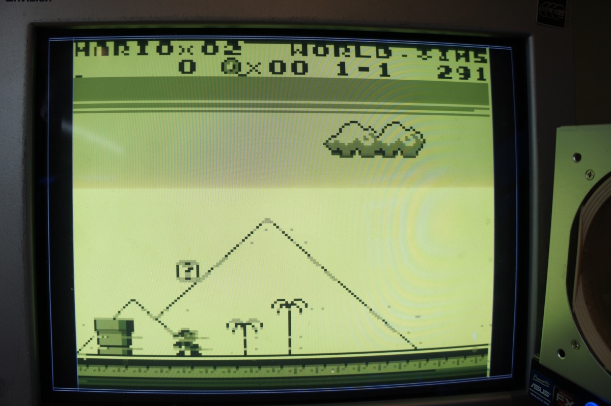
Currently the Gameboy LCD sniffer verilog code is just pulling data from the LCD bus without worrying about the clocks and putting it into the display ram. Basically just testing the level shifters. They work! Should be able to bang out the rest of the code tomorrow.
This is the project that the DE0 Digital IO Wing is for. I will use the IO wing to level shift the signals from the Gameboy’s LCD screen so my DE0 can capture the data. The Gameboy is a 5V device and the DE0 does not have 5V tolerant IO. I am using a SN74LVC8T245PWR 8-bit directional level shifter to do the translation on the IO wing board.
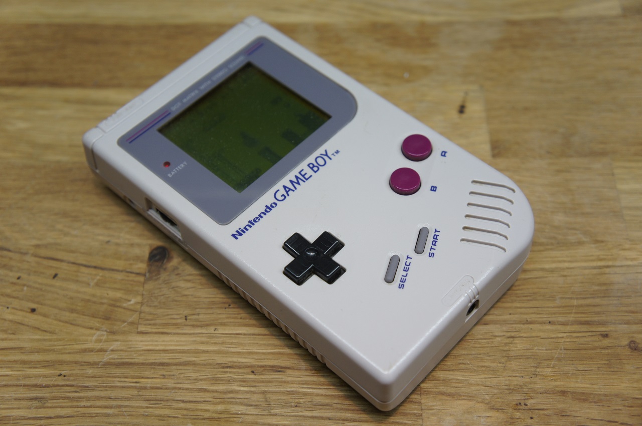
Purchased a Gameboy DMG-01 off eBay for $20. Needed some cleaning but it worked and had the battery cover!
The Gameboy DMG-01 uses triwing screws. Kidna like philips heads but with 3 “wings” instead of 4. Tool can be found on eBay or Amazon.
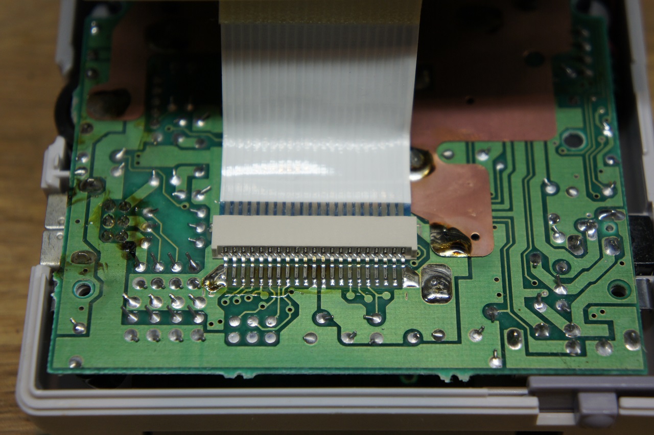
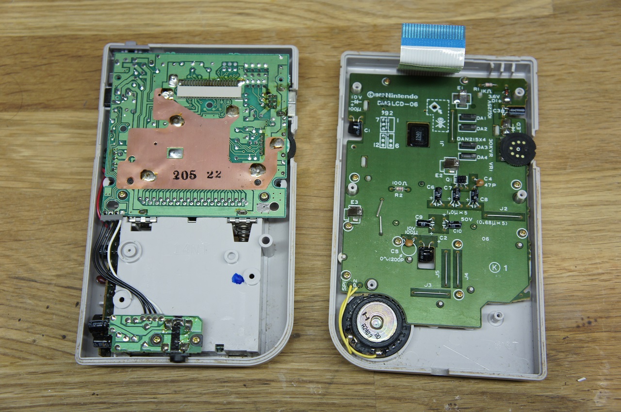
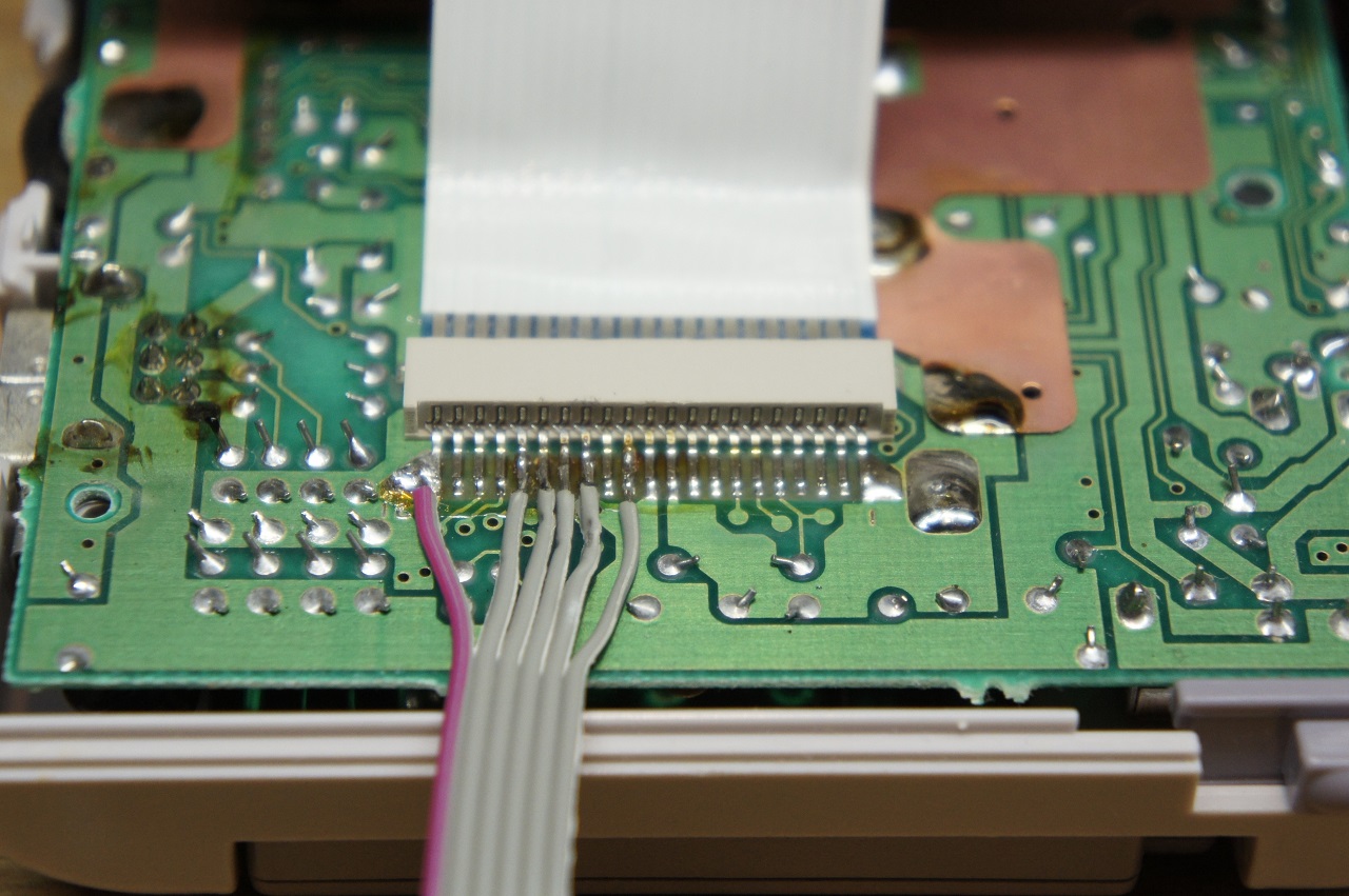
The connector between the front and back of the Gameboy is where I will tap into the signals to sneak a peak. Pinout is the following
Pin 12 – V-Sync
Pin 14 – Pixel Clock
Pin 15 – LCD Data 0
Pin 16 – LCD Data 1
Pin 17 – H-Sync
Pin 21 – Ground
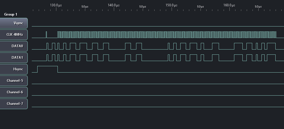
V-Sync should be 60Hz, Pixel Clock 4Mhz, and H-Sync 9.2kHz.
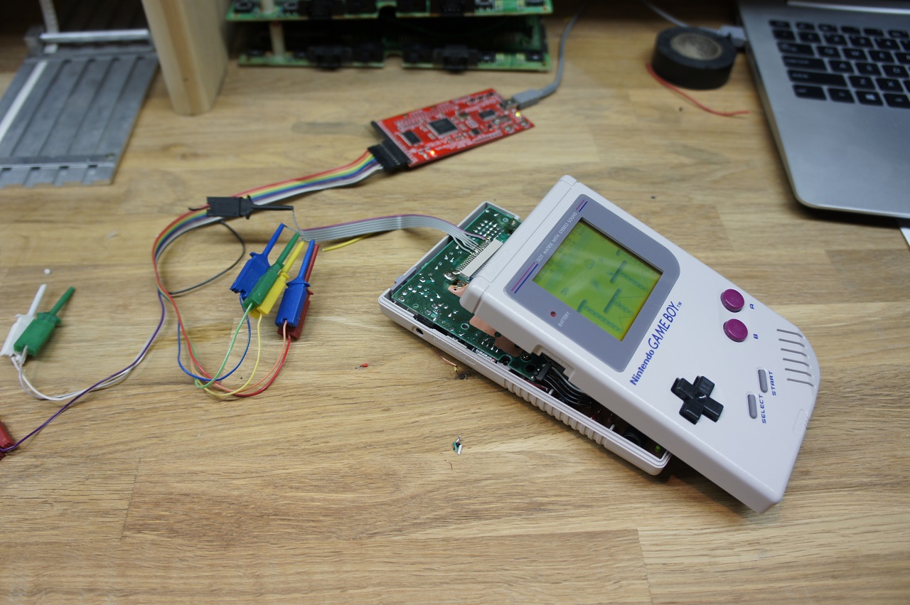
Connected up the Open Bench Logic Sniffer and powered up the Gameboy with a game in it then ran the capture. I had the trigger set to wait for the V-Sync signal.


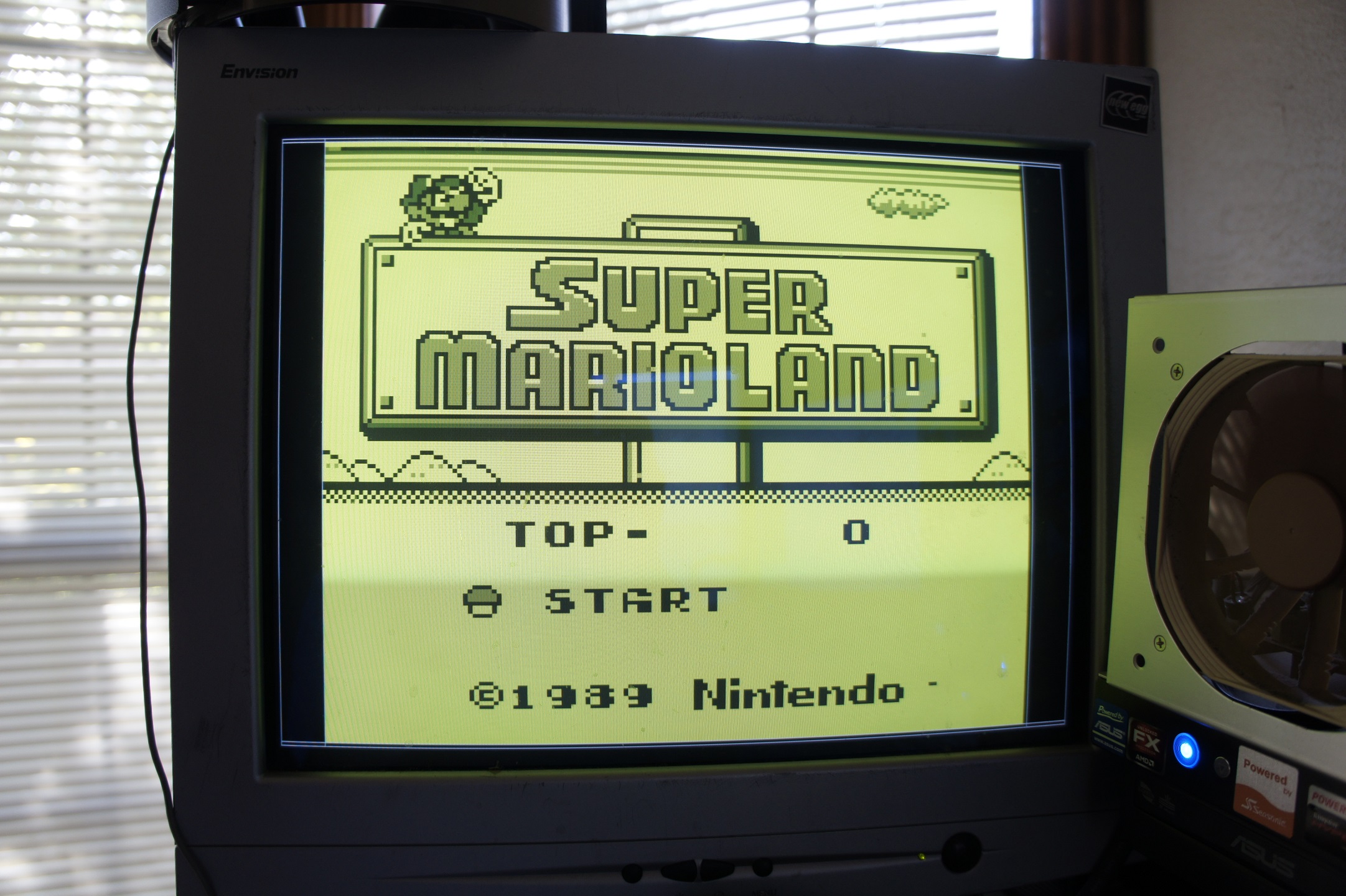
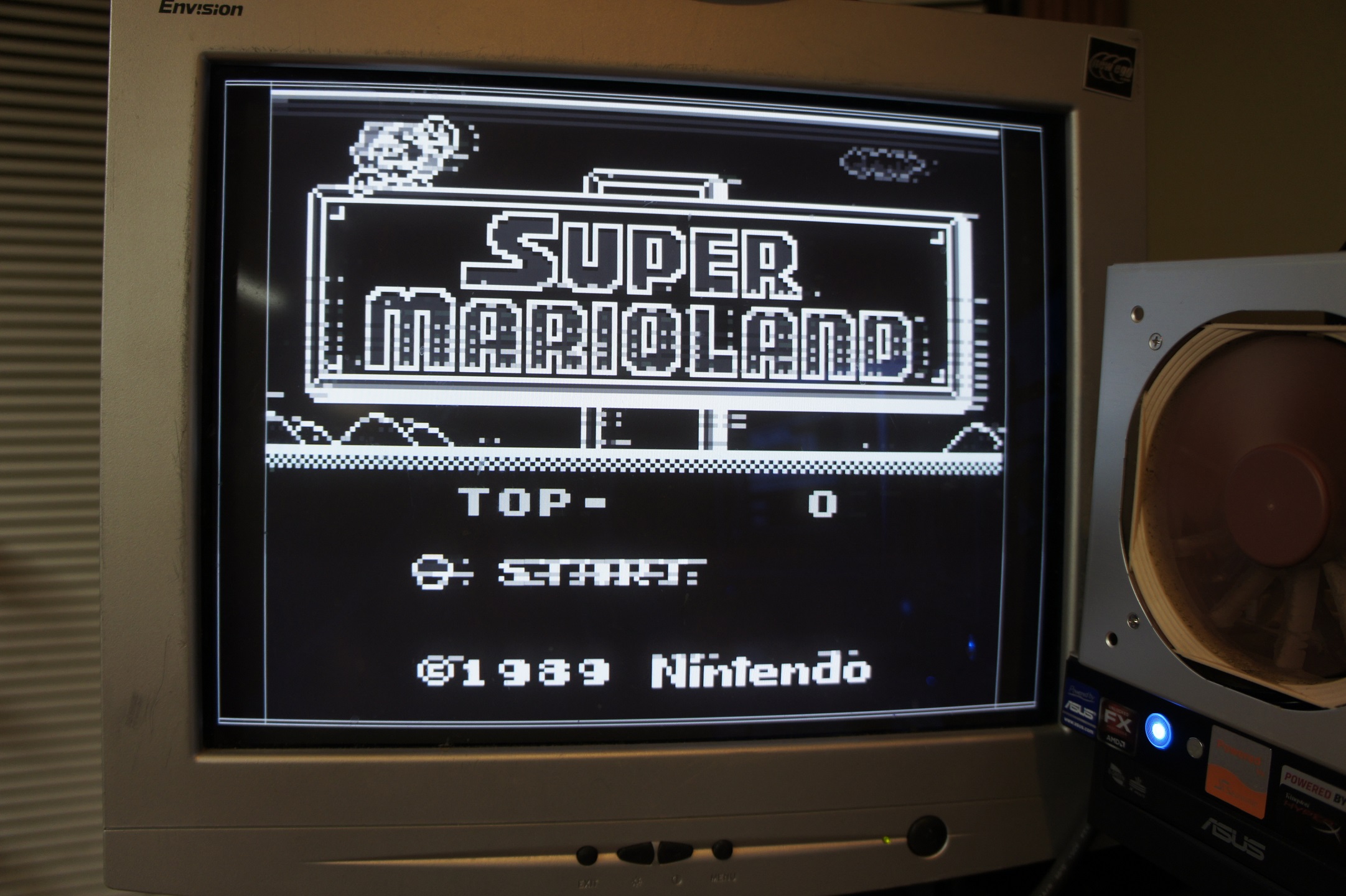
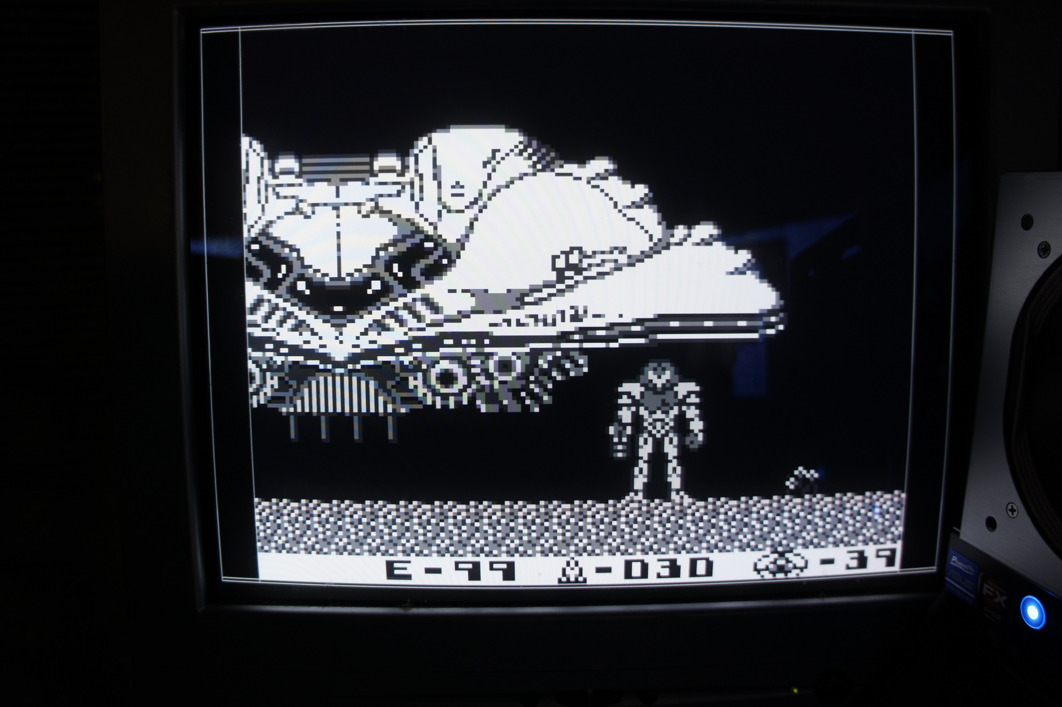
Then using my DE0_VGA_Driver I started writing the code take data from RAM on the FPGA and output it on the VGA monitor. I wrote a bitmap to .mif format (memory initialization file) convertor to display some Gameboy screenshots on the VGA Monitor. Link to that repo is here.
Currently working on getting the SN74LVC8T245PWR level shifters working and I will be able to pull live data from the Gameboy LCD data bus.
Working on a video driver for the Altera DE0 Development Board by terasIC. The DE0 has a 12bit (4bit per color) resistor ladder DAC that connects to the VGA connector. It is capable of 1280×1024 @ 60Hz officially but I think more is possible.
Find the files in the github repository.
