
Fixed an old bug in some RESET VECTOR DMD display code for multiple lines and got the above demo working. I will have to port the prop code to python however to make my twitter wall thingy.

Fixed an old bug in some RESET VECTOR DMD display code for multiple lines and got the above demo working. I will have to port the prop code to python however to make my twitter wall thingy.
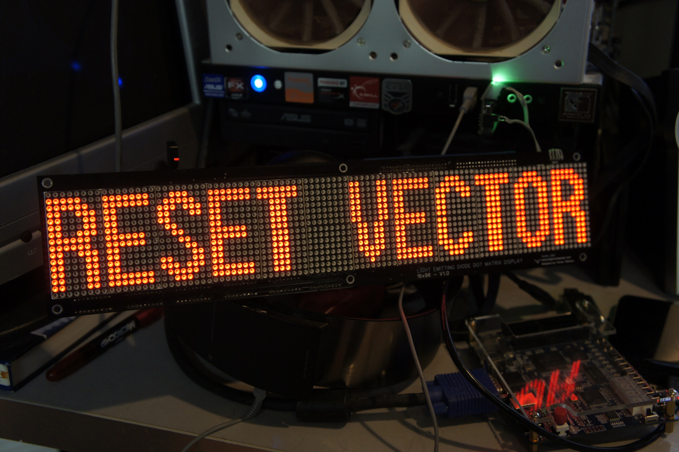
Pulled RESET VECTOR’s 96×16 DMD out of the parts bin and managed to find the old code to get it working again. Going to turn it into a Twitter Feed/Clock/Weather wall thing.
So I was still getting glitches on my inputs for Reset_Vector. I couldn’t figure out what was causing it because it would happen randomly and I couldn’t repeat the problem. The false inputs caused issues with ball triggering, score detection, and playfield actions. I figured it had to be glitches on the lines caused by EMF or something on the input driver. I knew it was the input driver cause when a solenoid fired randomly like the pop bumper it would register a hit which means that the microcontroller detected a hit.
To fix this issue I added a simple debouncer routine. Basically it makes sure a input is pressed for at least 2 Kernel cycles before saying that it was a hit. This keeps random spikes from registering as hits.
What it does is read in the inputs into a variable called new_inputs. The new_inputs then gets anded with a variable called old_inputs and the result is the inputs that where held for two kernel cycles. Then the new_inputs is copied into old_inputs for the next cycle to happen.
This system can be easily expanded to 3,4,ect cycles so the debouncer is extremely configurable in its sensitivity.
While developing the larger 36×128 DMD I ran out of registers and logic elements in the FPGA I was using. I could have switched to a larger FPGA but that would put the final product out of the price range I was aiming for. FPGAs have loads of dedicated ram so I decided to move the display memory from registers to a chunk of block ram. To test to see if the RAM code works I wrote a program for the 16×96 display in RESET_VECTOR. It took a bit of tweaking as I have never used block ram before but I was able to get it working.
module LED_Matrix_16x96
(
clk,row,col,SDRAM_CS,SRAM_CS,LAT,INPUT,SCLK
);
input wire clk;
input wire LAT;
input wire INPUT;
input wire SCLK;
output reg [0:15] row;
output reg [95:0] col;
output reg [0:0] SDRAM_CS;
output reg [0:0] SRAM_CS;
reg [24:0] clk_slow;
reg [4:0] row_cnt;
reg [1535:0] col_buffer;
reg [3:0] read_addr;
reg [3:0] write_addr;
reg [95:0] disp_mem_data;
reg disp_mem_wren;
wire [95:0] disp_mem_q;
reg [3:0] sel;
initial
begin
row <= 16'b0000000000000001;
col <= 16'b0000000000000000;
SDRAM_CS <= 1'b0;
SRAM_CS <= 1'b0;
clk_slow <= 16'b0000000000000000;
row_cnt <= 5'b00000;
write_addr <= 4'b0000;
read_addr <= 4'b0000;
disp_mem_wren <= 0;
sel <= 4'b0000;
end
always @(posedge clk)
begin
clk_slow <= clk_slow + 1'b1;
if(!LAT & row_cnt == 5'b01111)
begin
case(sel)
4'b0000:
begin
write_addr <= sel;
disp_mem_wren <= 1'b1;
disp_mem_data <= col_buffer[1535:1440];
sel <= 4'b0001;
end
4'b0001:
begin
write_addr <= sel;
disp_mem_wren <= 1'b1;
disp_mem_data <= col_buffer[1439:1344];
sel <= 4'b0010;
end
4'b0010:
begin
write_addr <= sel;
disp_mem_wren <= 1'b1;
disp_mem_data <= col_buffer[1343:1248];
sel <= 4'b0011;
end
4'b0011:
begin
write_addr <= sel;
disp_mem_wren <= 1'b1;
disp_mem_data <= col_buffer[1247:1152];
sel <= 4'b0100;
end
4'b0100:
begin
write_addr <= sel;
disp_mem_wren <= 1'b1;
disp_mem_data <= col_buffer[1151:1056];
sel <= 4'b0101;
end
4'b0101:
begin
write_addr <= sel;
disp_mem_wren <= 1'b1;
disp_mem_data <= col_buffer[1055:960];
sel <= 4'b0110;
end
4'b0110:
begin
write_addr <= sel;
disp_mem_wren <= 1'b1;
disp_mem_data <= col_buffer[959:864];
sel <= 4'b0111;
end
4'b0111:
begin
write_addr <= sel;
disp_mem_wren <= 1'b1;
disp_mem_data <= col_buffer[863:768];
sel <= 4'b1000;
end
4'b1000:
begin
write_addr <= sel;
disp_mem_wren <= 1'b1;
disp_mem_data <= col_buffer[767:672];
sel <= 4'b1001;
end
4'b1001:
begin
write_addr <= sel;
disp_mem_wren <= 1'b1;
disp_mem_data <= col_buffer[671:576];
sel <= 4'b1010;
end
4'b1010:
begin
write_addr <= sel;
disp_mem_wren <= 1'b1;
disp_mem_data <= col_buffer[575:480];
sel <= 4'b1011;
end
4'b1011:
begin
write_addr <= sel;
disp_mem_wren <= 1'b1;
disp_mem_data <= col_buffer[479:384];
sel <= 4'b1100;
end
4'b1100:
begin
write_addr <= sel;
disp_mem_wren <= 1'b1;
disp_mem_data <= col_buffer[383:288];
sel <= 4'b1101;
end
4'b1101:
begin
write_addr <= sel;
disp_mem_wren <= 1'b1;
disp_mem_data <= col_buffer[287:192];
sel <= 4'b1110;
end
4'b1110:
begin
write_addr <= sel;
disp_mem_wren <= 1'b1;
disp_mem_data <= col_buffer[191:96];
sel <= 4'b1111;
end
4'b1111:
begin
write_addr <= sel;
disp_mem_wren <= 1'b1;
disp_mem_data <= col_buffer[95:0];
sel <= 4'b0000;
end
default:
begin
sel <= 4'b0000;
write_addr <= 4'b0000;
disp_mem_wren <= 1'b0;
end
endcase
end
else
begin
disp_mem_wren <= 1'b0;
sel <= 4'b0000;
end
end
always @(posedge clk_slow[10])
begin
if(row_cnt > 5'b01111)
begin
row_cnt <= 5'b00000;
end
col <= disp_mem_q;
row_cnt <= row_cnt + 1'b1;
row <= {row[15],row[0:14]};
read_addr <= read_addr + 1'b1;
end
always @(posedge SCLK)
begin
if(LAT)
begin
col_buffer <= {col_buffer[1534:0],INPUT};
end
end
display_ram disp_mem_inst (
.rdaddress (read_addr),
.wraddress (write_addr),
.clock (clk),
.data (disp_mem_data),
.wren (disp_mem_wren),
.q (disp_mem_q)
);
endmodule
Sorry for the massive amount of code recently. To test to see if the RAM code works I wrote a program for the 16×96 display in RESET_VECTOR. If this works then I will order the PCB for the 32×128 DMD. If anyone has any suggestions please feel free to comment. This is the first time I have tried interfacing RAM on an FPGA before.
module LED_Matrix_16x96
(
clk,row,col,SDRAM_CS,SRAM_CS,LAT,INPUT,SCLK
);
input  wire    clk;
input  wire    LAT;
input  wire    INPUT;
input  wire    SCLK;

output  reg [0:15]  row;
output  reg [95:0]  col;
output  reg [0:0]   SDRAM_CS;
output  reg [0:0]   SRAM_CS;

reg [24:0]  clk_slow;
reg [4:0]  row_cnt;
reg [1535:0]  col_buffer;

reg  [3:0]  read_addr;
reg  [3:0]  write_addr;
reg  [95:0]  disp_mem_data;
reg      disp_mem_wren;
wire  [95:0]  disp_mem_q;

reg [3:0]  sel;
initial
begin
row <= 16'b0000000000000001;
    col <= 16'b0000000000000000;
    SDRAM_CS <= 1'b0;
    SRAM_CS <= 1'b0;
    clk_slow <= 16'b0000000000000000;
    row_cnt <= 5'b00000;
    write_addr <= 4'b0000;
    read_addr <= 4'b0000;
    disp_mem_wren <= 0;
    sel <= 4'b0000;
  end

always @(posedge clk)
begin
  clk_slow <= clk_slow + 1'b1;

  if(!LAT & row_cnt == 5'b01111)
  begin
  case(sel)
    4'b0000:
    begin
      write_addr <= sel;
      disp_mem_wren <= 1'b1;
      disp_mem_data <= col_buffer[1535:1440];
      sel <= 4'b0001;
    end
    4'b0001:
    begin
      write_addr <= sel;
      disp_mem_wren <= 1'b1;
      disp_mem_data <= col_buffer[1439:1344];
      sel <= 4'b0010;
    end
    4'b0010:
    begin
      write_addr <= sel;
      disp_mem_wren <= 1'b1;
      disp_mem_data <= col_buffer[1343:1248];
      sel <= 4'b0011;
    end
    4'b0011:
    begin
      write_addr <= sel;
      disp_mem_wren <= 1'b1;
      disp_mem_data <= col_buffer[1247:1152];
      sel <= 4'b0100;
    end
    4'b0100:
    begin
      write_addr <= sel;
      disp_mem_wren <= 1'b1;
      disp_mem_data <= col_buffer[1151:1056];
      sel <= 4'b0101;
    end
    4'b0101:
    begin
      write_addr <= sel;
      disp_mem_wren <= 1'b1;
      disp_mem_data <= col_buffer[1055:960];
      sel <= 4'b0110;
    end
    4'b0110:
    begin
      write_addr <= sel;
      disp_mem_wren <= 1'b1;
      disp_mem_data <= col_buffer[959:864];
      sel <= 4'b0111;
    end
    4'b0111:
    begin
      write_addr <= sel;
      disp_mem_wren <= 1'b1;
      disp_mem_data <= col_buffer[863:768];
      sel <= 4'b1000;
    end
    4'b1000:
    begin
      write_addr <= sel;
      disp_mem_wren <= 1'b1;
      disp_mem_data <= col_buffer[767:672];
      sel <= 4'b1001;
    end
    4'b1001:
    begin
      write_addr <= sel;
      disp_mem_wren <= 1'b1;
      disp_mem_data <= col_buffer[671:576];
      sel <= 4'b1010;
    end
    4'b1010:
    begin
      write_addr <= sel;
      disp_mem_wren <= 1'b1;
      disp_mem_data <= col_buffer[575:480];
      sel <= 4'b1011;
    end
    4'b1011:
    begin
      write_addr <= sel;
      disp_mem_wren <= 1'b1;
      disp_mem_data <= col_buffer[479:384];
      sel <= 4'b1100;
    end
    4'b1100:
    begin
      write_addr <= sel;
      disp_mem_wren <= 1'b1;
      disp_mem_data <= col_buffer[383:288];
      sel <= 4'b1101;
    end
    4'b1101:
    begin
      write_addr <= sel;
      disp_mem_wren <= 1'b1;
      disp_mem_data <= col_buffer[287:192];
      sel <= 4'b1110;
    end
    4'b1110:
    begin
      write_addr <= sel;
      disp_mem_wren <= 1'b1;
      disp_mem_data <= col_buffer[191:96];
      sel <= 4'b1111;
    end
    4'b1111:
    begin
      write_addr <= sel;
      disp_mem_wren <= 1'b1;
      disp_mem_data <= col_buffer[95:0];
      sel <= 4'b0000;
    end
    default:
    begin
      sel <= 4'b0000;
      write_addr <= 4'b0000;
      disp_mem_wren <= 1'b0;
    end
  endcase
  end
  else
  begin
    disp_mem_wren <= 1'b0;
    sel <= 4'b0000;
  end
end

always @(posedge clk_slow[10])
begin
  if(row_cnt > 5'b01111)
begin
row_cnt <= 5'b00000;
  end
  col <= disp_mem_q;
  row_cnt <= row_cnt + 1'b1;
  row <= {row[15],row[0:14]};
  read_addr <= read_addr + 1'b1;

end

always @(posedge SCLK)
begin
  if(LAT)
  begin
    col_buffer <= {col_buffer[1534:0],INPUT};
  end
end

display_ram disp_mem_inst (
        .rdaddress (read_addr),
        .wraddress (write_addr),
        .clock  (clk),
        .data   (disp_mem_data),
        .wren   (disp_mem_wren),
        .q      (disp_mem_q)
);

endmodule
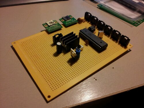
A work in progress. Some of the new features include a socketable Propeller Chip, lockable headers, and separate power lines for the microcontroller and other sub systems. These changes will make the system easier to fix and prevent future problems.
I finally finished building the Dot Matrix Display for Reset Vector. The Matrixing is run by a FPGA. The data is shifted in by the main propeller microcontroller. Currently the only code on the propeller is the single line text generator. I have a double line text generator and a animation driver that will load bitmaps off an SD card.
The Code will be up tomorrow.
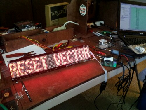
Just got it working.
I soldered on what parts I had on hand and got the DMD display working today. Will upload the code after I get all the modules soldered on.

Just finished the DMD (Dot Matrix Display) test for RESET_VECTOR. Since the Propeller is to slow to do the matrixing I am going to use a FPGA to do it. The propeller will send the data over a serial connection into a frame buffer on the FPGA. When all the data is on the FPGA the FPGA will update its matrixing buffer.
I have the Propeller to FPGA communication protocol written and tested as well. The Propeller loads the Data off the SD card and sends it serially to the FPGA.
Propeller Code
FPGA Code
Block Diagram of the Dot Matrix.
