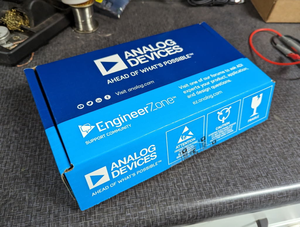
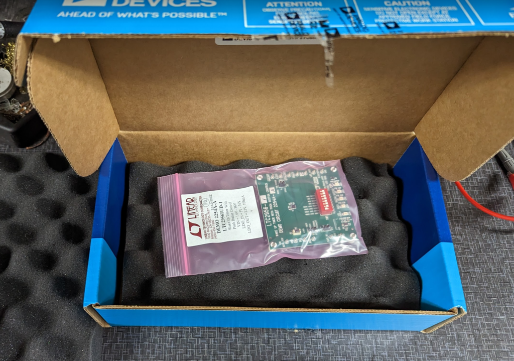
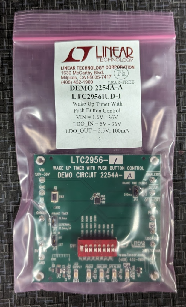
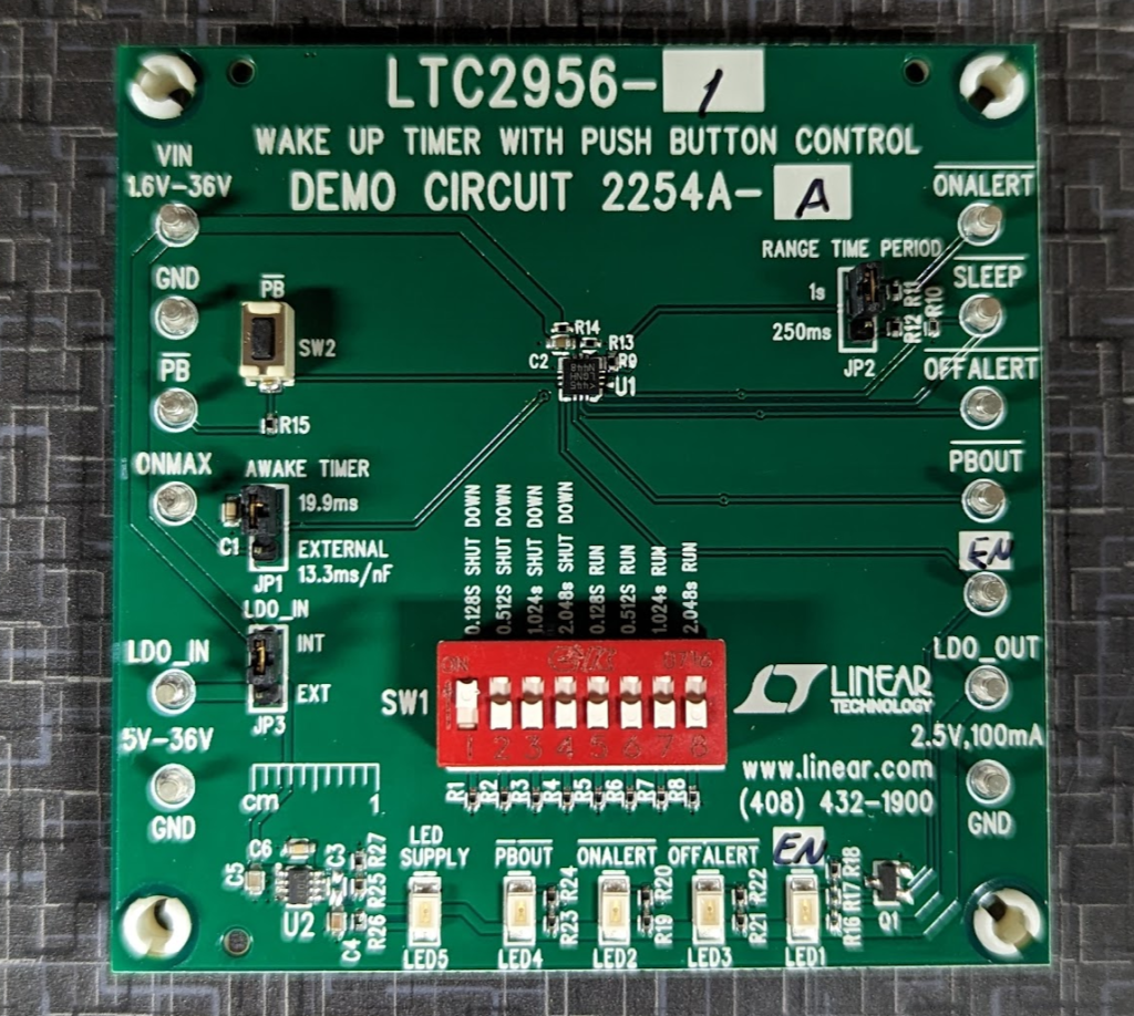
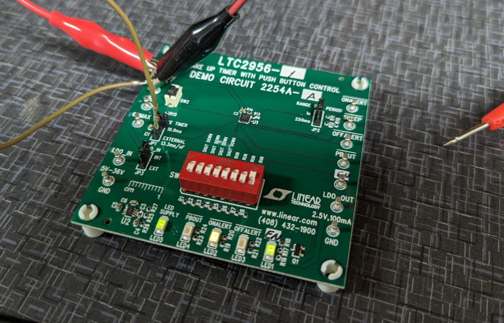
For keeping the time for the Cat Feeder Unreminder I am planning on using the LTC2956-1 which is a super low power timer that has push button reset control. It can accurately handle very long timers that a traditional RC style timers (think 555 timer) wouldn’t be able to do.
For my use case, I am going to pull ONMAX to GND which will disable the timer that turns off the AWAKE timer. I will toggle the Sleep pin from low to high to low to reset the timer.
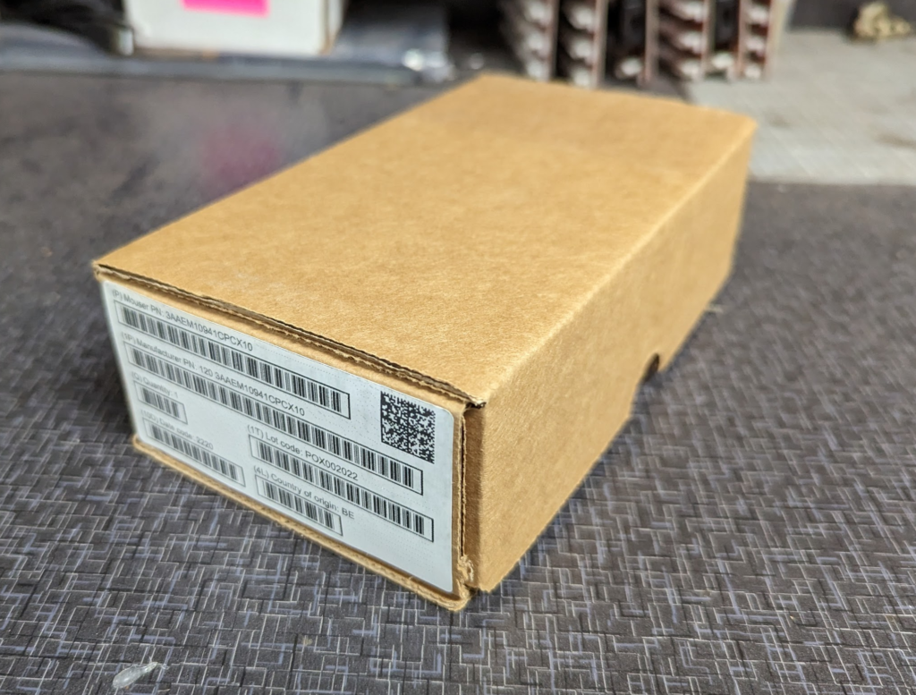
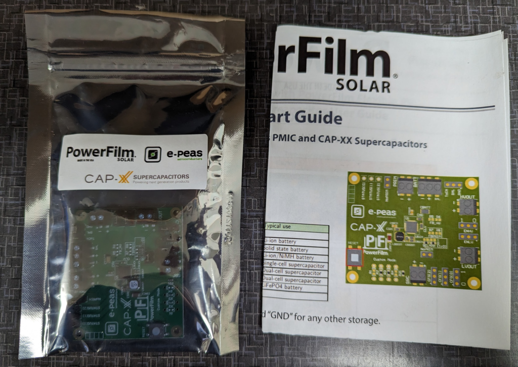
Received the 3AAEM10941CPCX10 evaluation kit for the AEM10941 solar harvesting chip today.
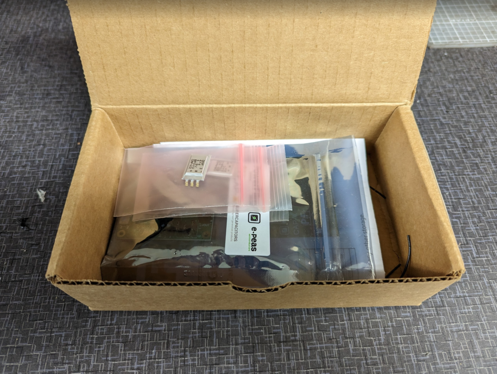
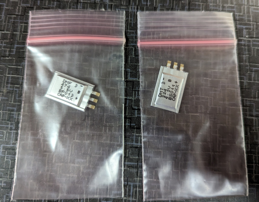
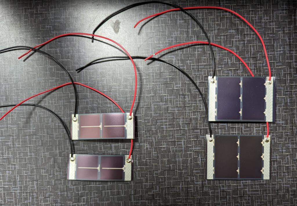
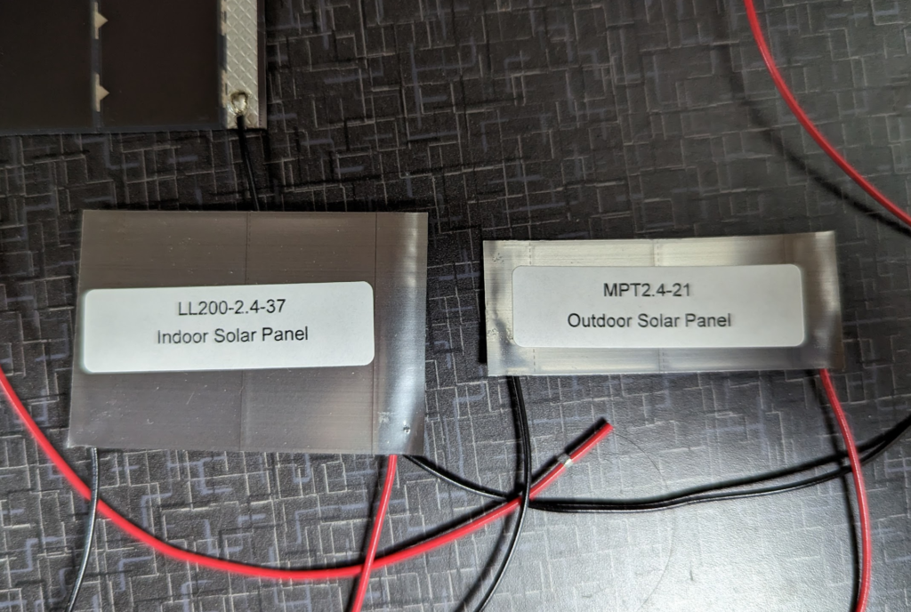
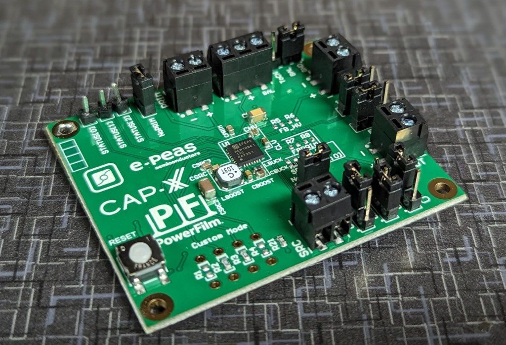
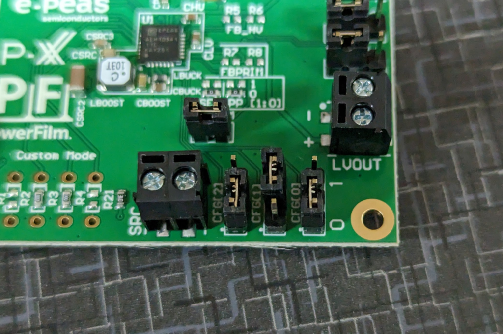
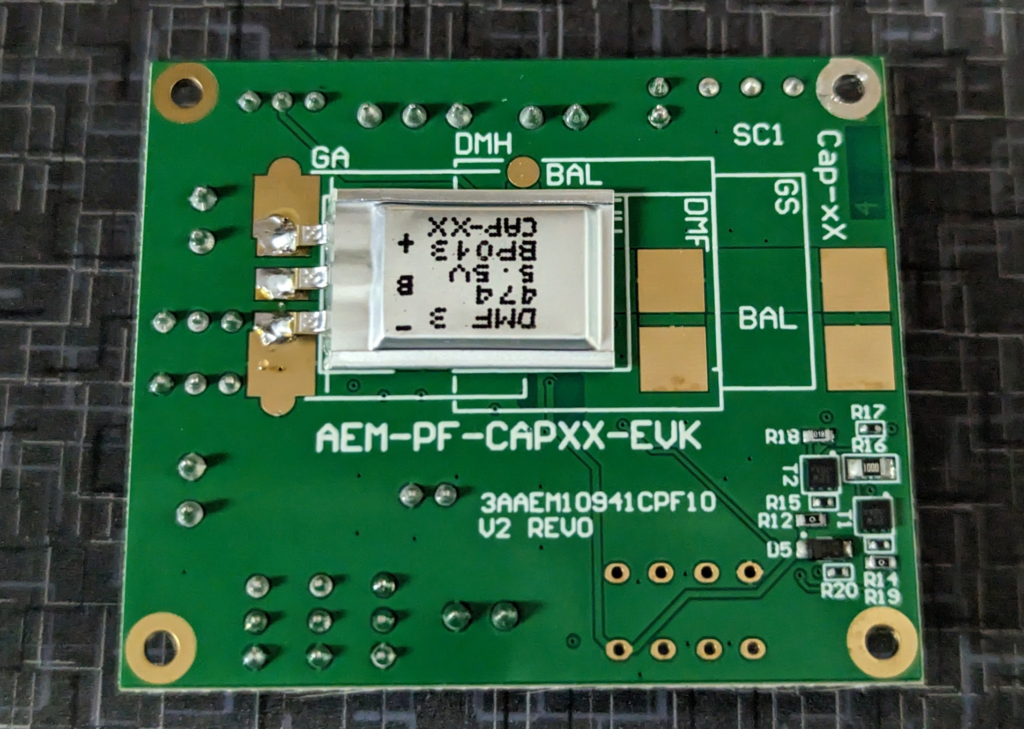
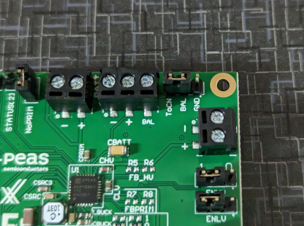
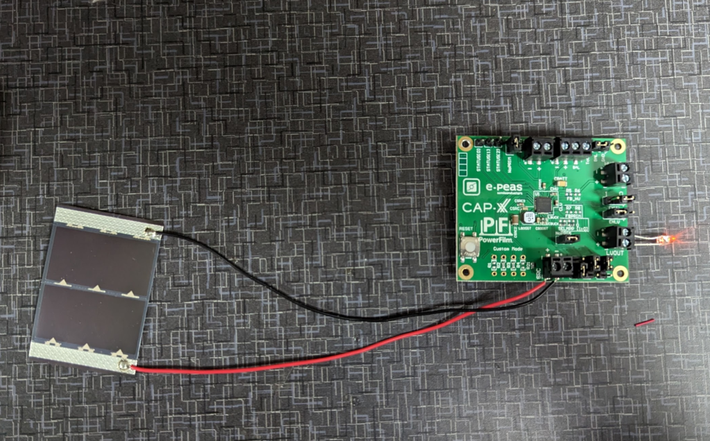
Box the kit came in. Surprised how “plain” the box is. Usually manufactures for evaluation kits have fancy boxes with branding on it so it can be viewed from the engineer’s storage shelf ;) .Inside. There was some bubble wrap I removed to keep everything from being shaken around.The super caps that come with the kit. Part numbers: DMT3N4R2U224M3DTA0 and DMF3Z5R5H474M3DTA0.The demo board and quick start guide.Two different kinds of solar panels. An Outdoor (smaller size) and Inside (larger size) type of panel. Part numbers for the solar panels are LL200-2.4-37 for the indoor panel and MPT2.4-21 for the outdoor panel. From the little bit I know about solar panels is that these are probably tuned to the light frequencies of there environment. The demo board. Quality of assembly isn’t the best. Jumpers are not soldered straight. Biggest one is the STATUS[2] pin on the upper right of the board. Also, the board’s jumpers are not set out of the box for the given example. Annoying to say the least. First step on firing up the the demo board is to set these CFG pins. Shown is how mine arrived. You need to set the jumpers to CFG[2] = 0, CFG[1] = 1, and CFG[0] = 1.Next, solder one of the super capacitors to the back side of the board as shown. I used the DMF3Z5R5H474M3DTA0 which is the larger of the two. Set the BAL jumper to connect BAL to ToCN. BAL is the balance pin of the super capacitor. These super capacitors are actually two cells in series and the balance pin is the connection between the two.Then attach the solar panel to the SRC terminal. To see if there is voltage output I put a LED across the LVOUT. The LVOUT voltage regulator is set to 1.8V which is below the forward voltage of the LED I chose.
Its possible it won’t light up right away. It takes sometime for the super capacitor to charge up. You can charge up the super capacitor with a power supply set to 3.3V and current limited to around 10-20mA. Make sure to not reverse bias the charging!
Voltage across the super capacitor while charging up off the solar panel!
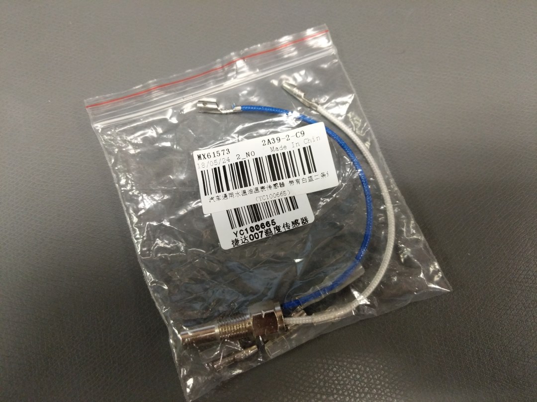
To read oil and coolant temperature on the Jeep I wanted to use automotive parts for the sensors. Most temperature sensors in the automotive world are thermistors. I searched around for some in 1/8″ NPT and found some designed for aftermarket gauges. Only problem was there was no datasheet for them…which is necessary to accurately read the thermistors since they are non linear devices. At under $4 a piece I ordered them anyways.
Thermistors with part number MX61573 and YC100665.
Fortunately when they arrived they had a part number on them and after some googling I managed to find a temperature chart.
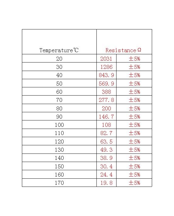
Temperature to resistance chart for the MX61573 Thermistors.
I double checked the values with a multimeter and setting the hot air gun to the temperatures in the chart above and seeing what the resistance was. Everything matched.
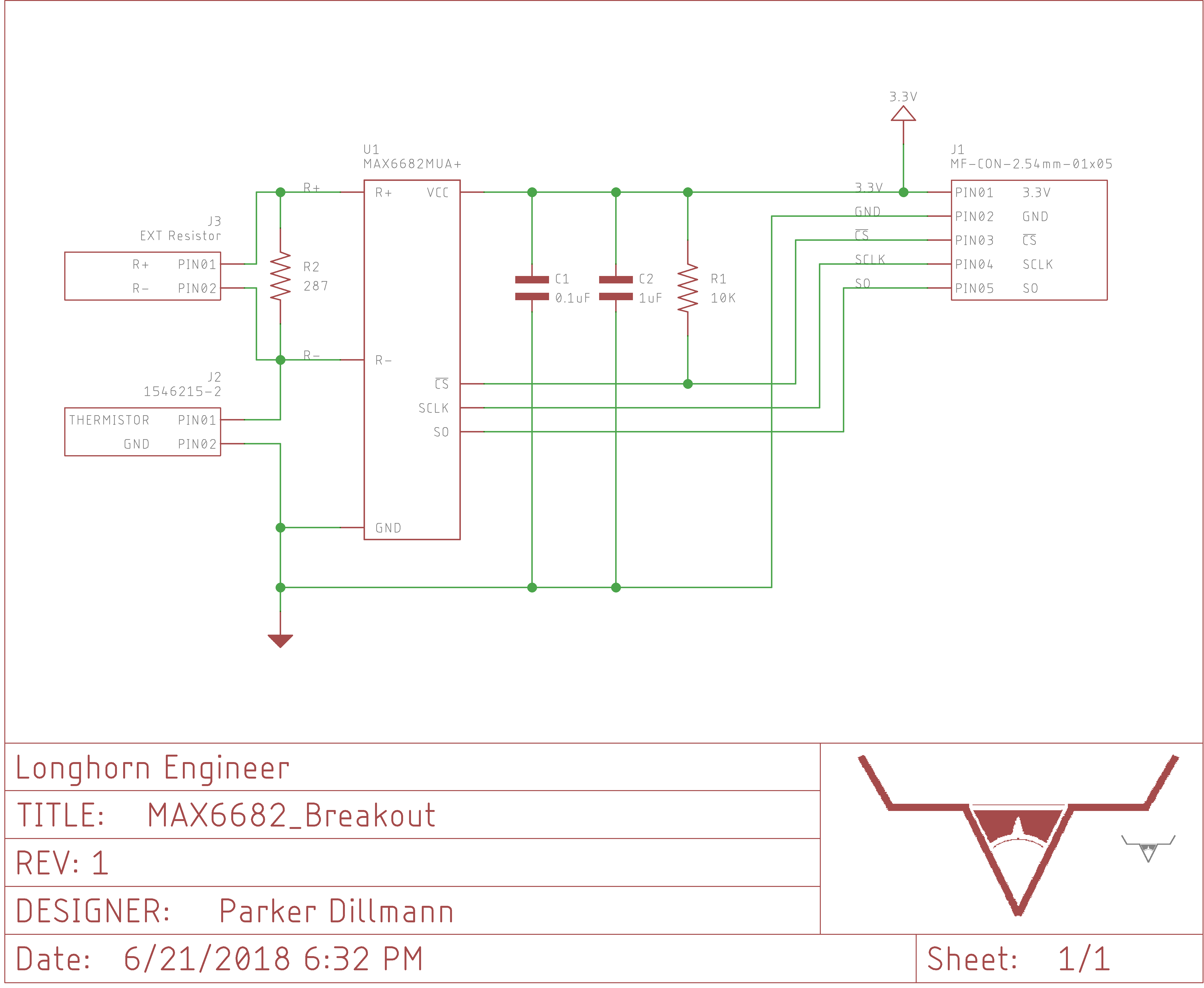
To read the thermistors I decided to use the MAX6682 IC. This IC gets rid of power supply noise and thermal self heating of the thermistor.
The only thing I had to calculate was the REXT value. I used the 2031 ohm (20C) for RMAX, 108 ohm (100C) for RMIN, and 388 ohm (60C) for RMID. This came out to a value of 287 ohms. Which the resistor ERA-3AEB2870V by Panasonic works. See page 6 of the datesheet for the formula to calculate REXT.
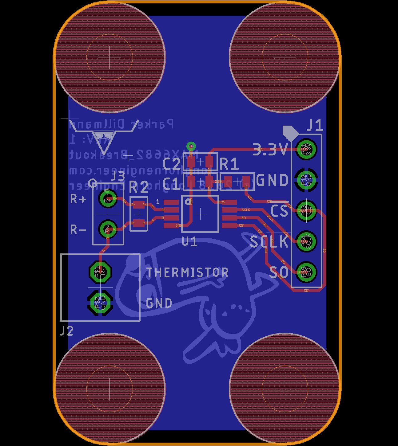
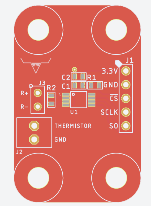
Then I drew up the schematic and layout for the breakout board.
Schematic for the MAX6682 Breakout Board.
Layout for the MAX6682 Breakout Board.
I added a little header (J3) that will allow me to easily change the REXT value for other thermistors.
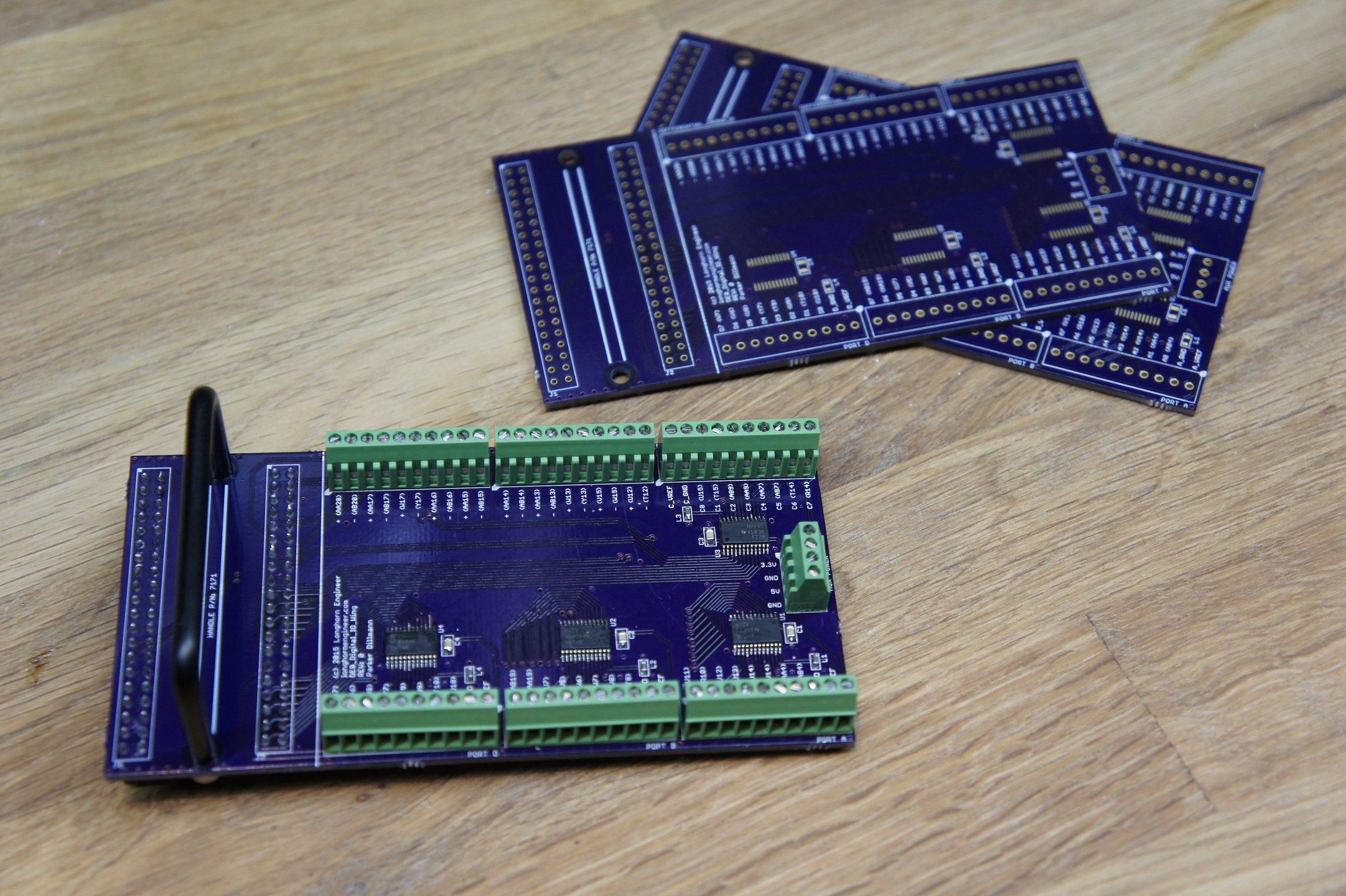
Boards and parts arrived today from OSH Park and Mouser. Soldered them up after work.
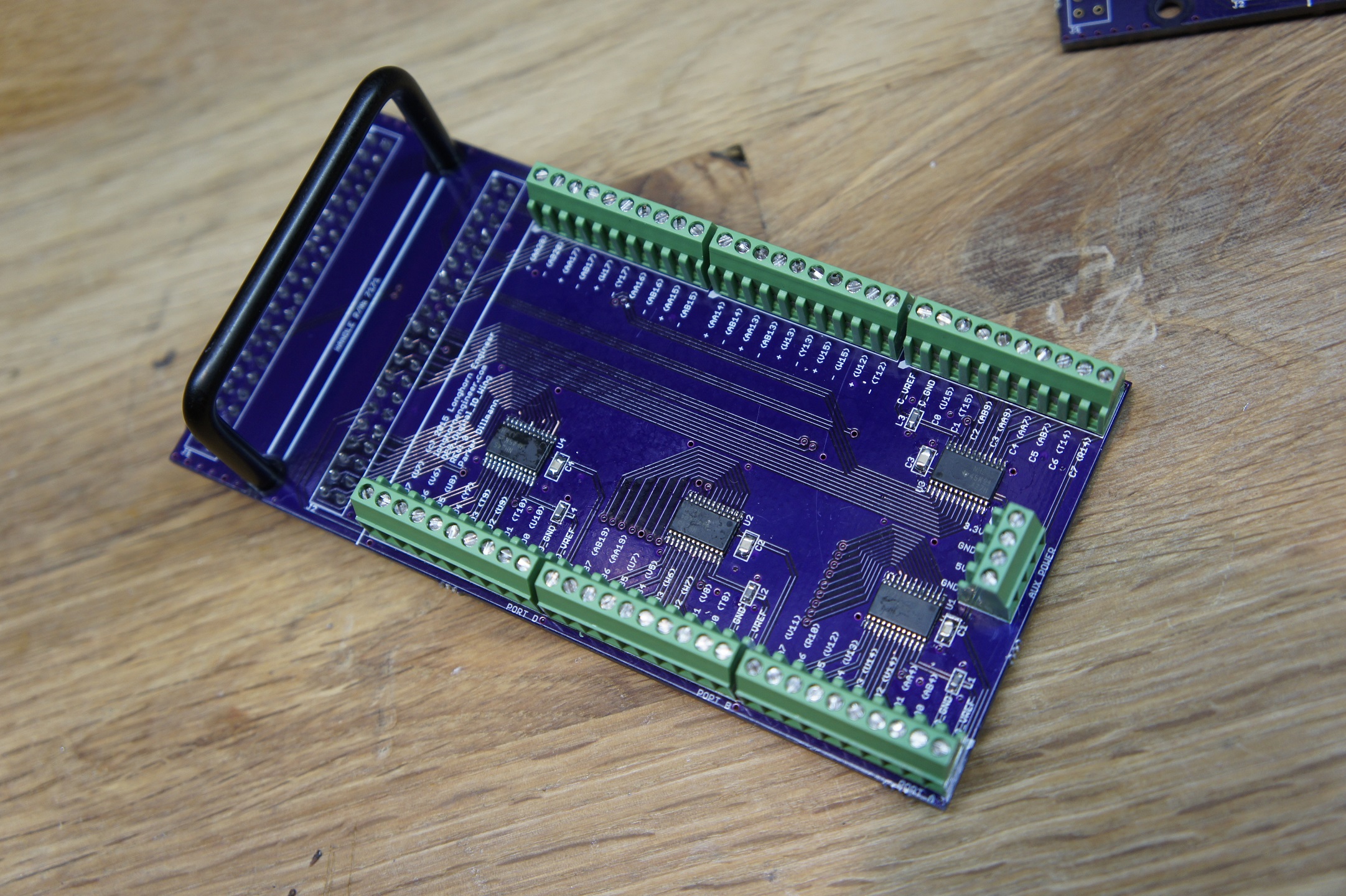
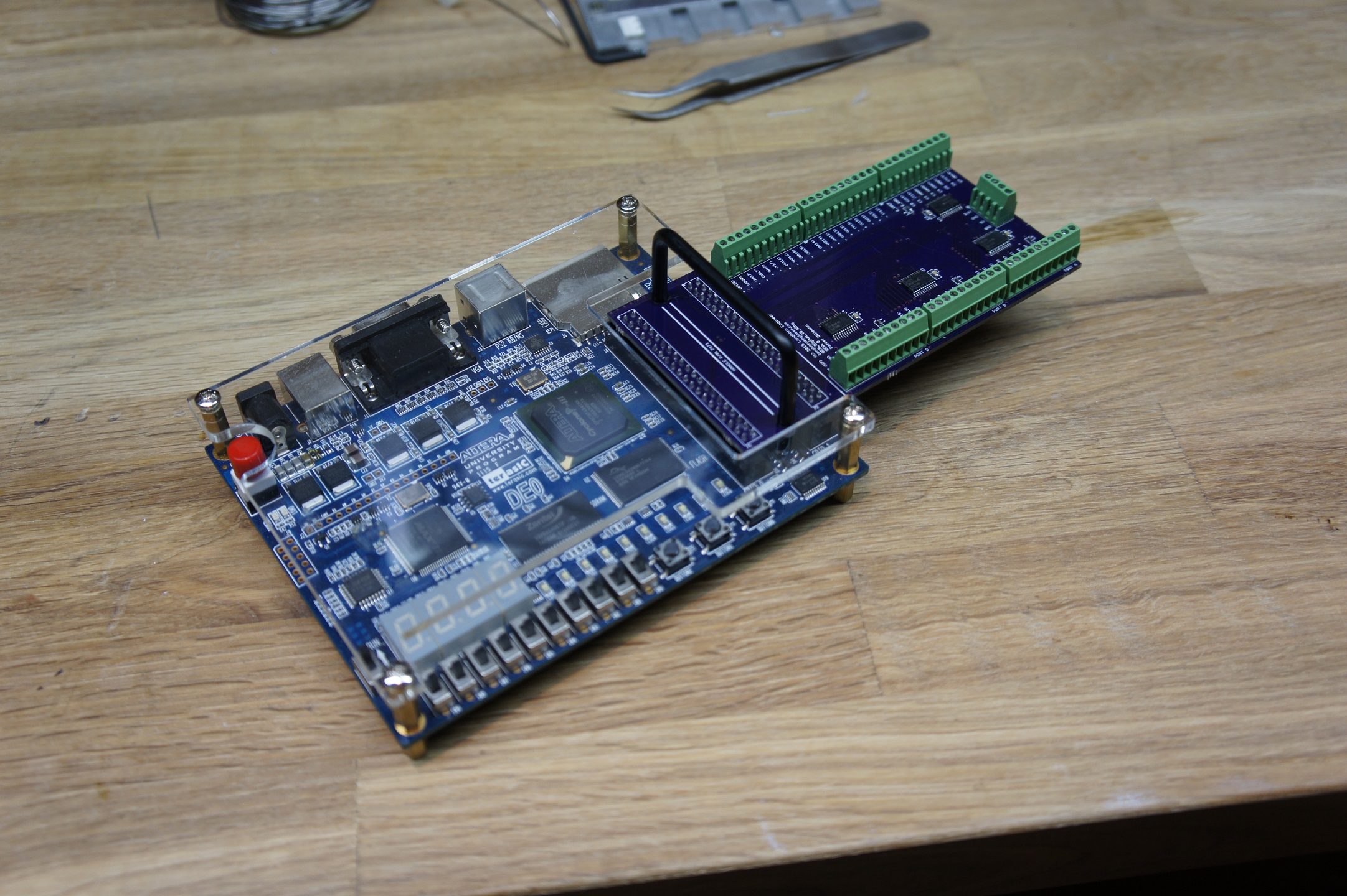
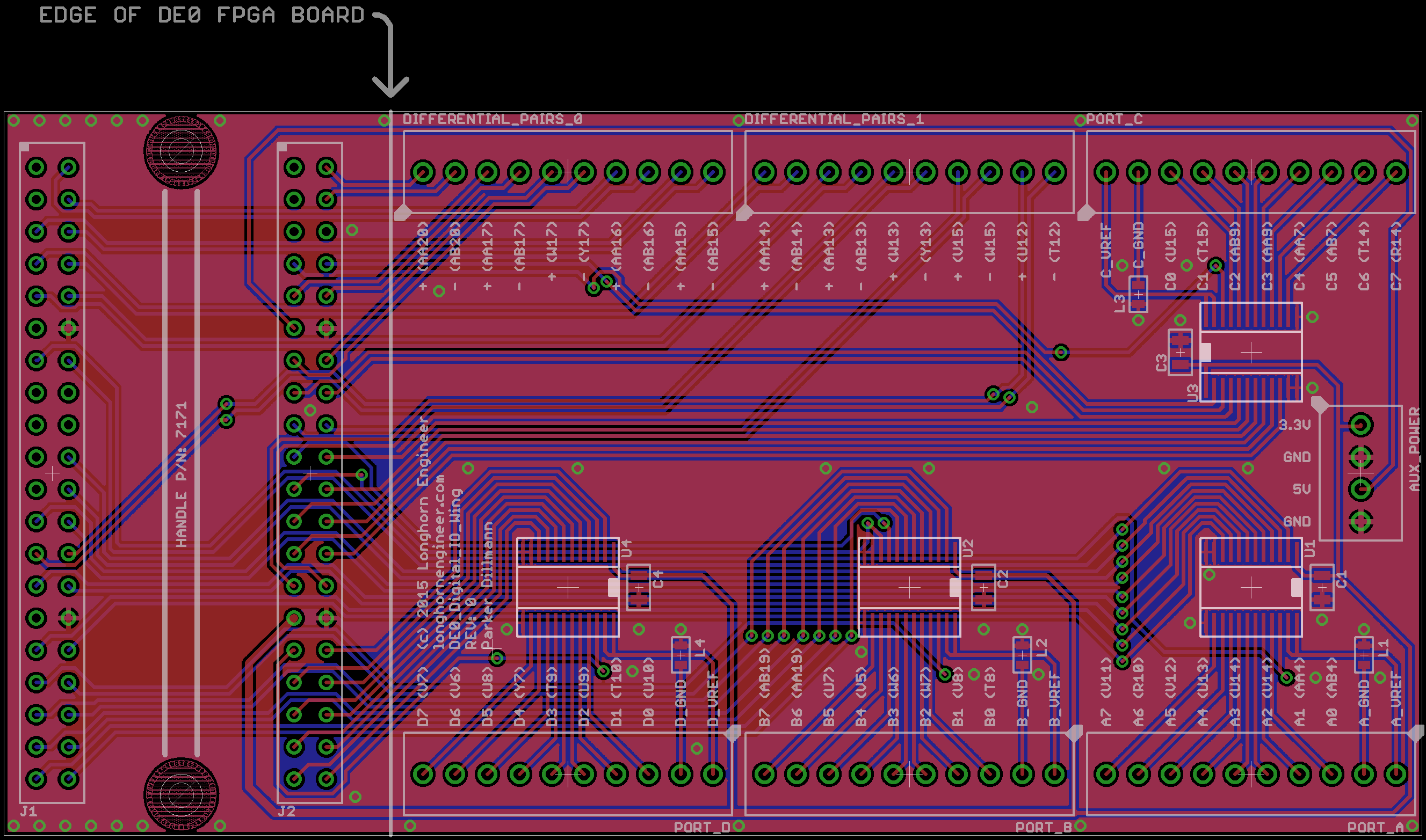
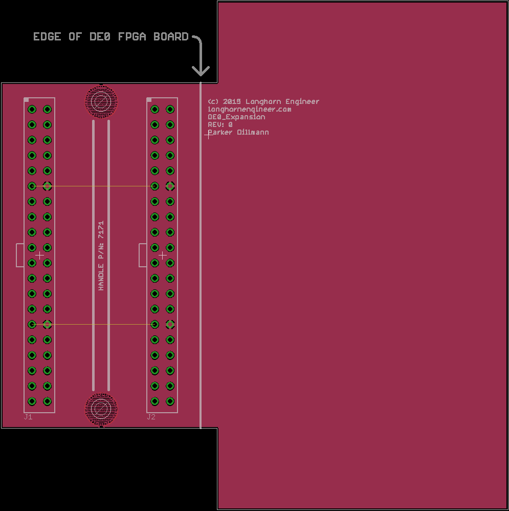
Close up of the board. Not a ton of parts…all connectors. The handle idea worked out pretty well. The board can be pulled out of the dual 40pin headers with ease!
Expansion mounted in the DE0 DEV board. Gotta write up some verilog to test it out now.
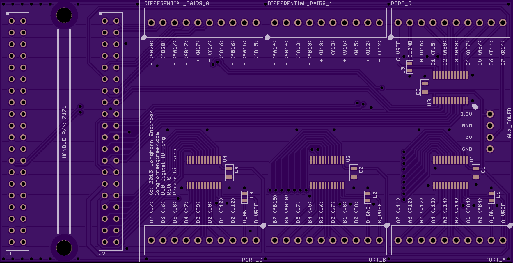
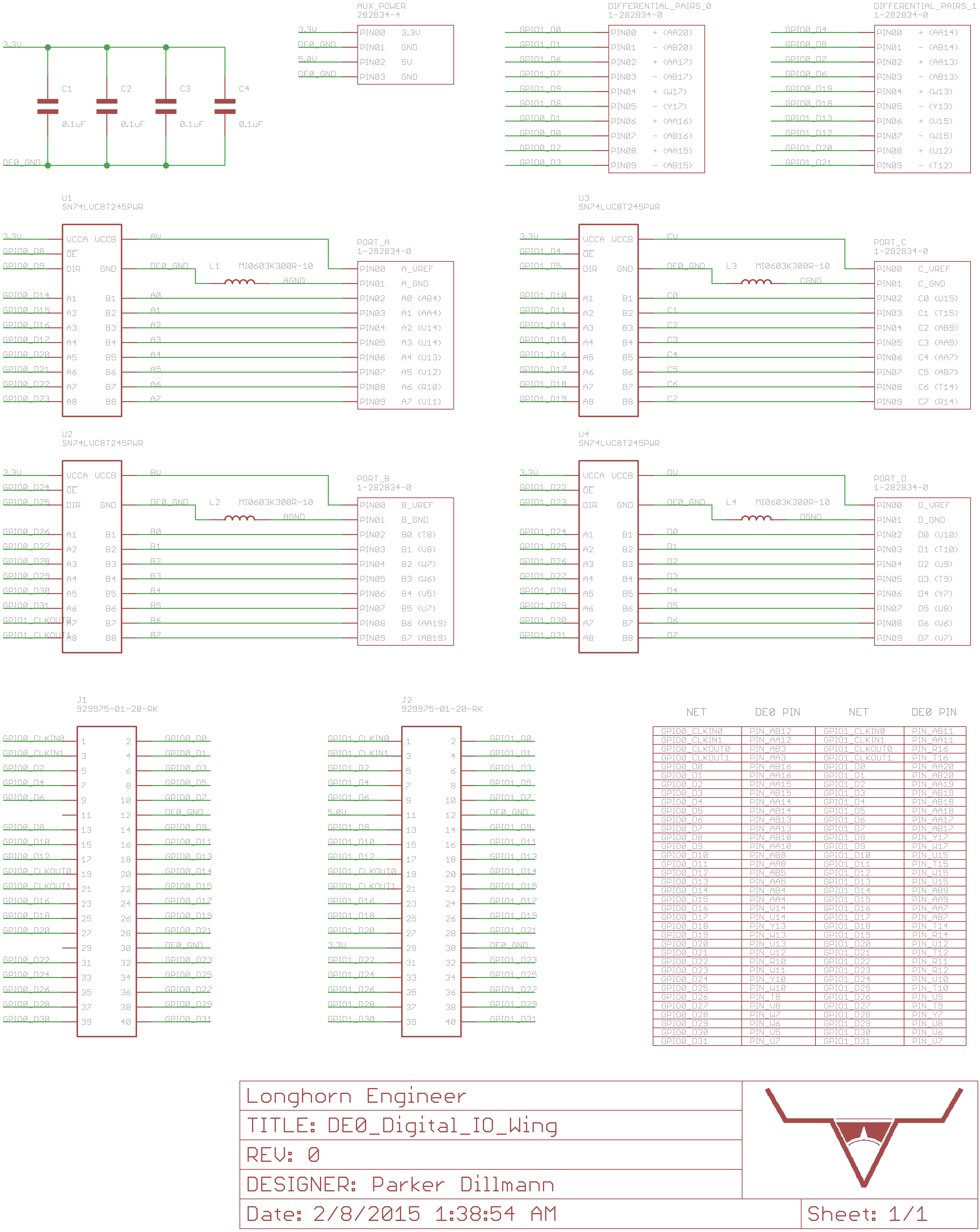
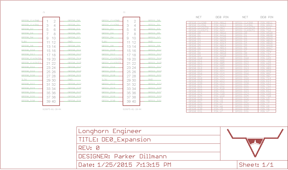
Design ended up having only 10 LVDS signals broken out as that required less unique parts. The connectors are expensive (1-282834-0) running ~$5.70 in singles. I will be looking into alternatives to see if I can get the cost down. I found some on AliExpress but I will need to order them and test them to see if they are any good.
I also included a 4 position auxiliary power connector to power up external circuits. No power safety though (fuses/TVS) so use at your own risk!
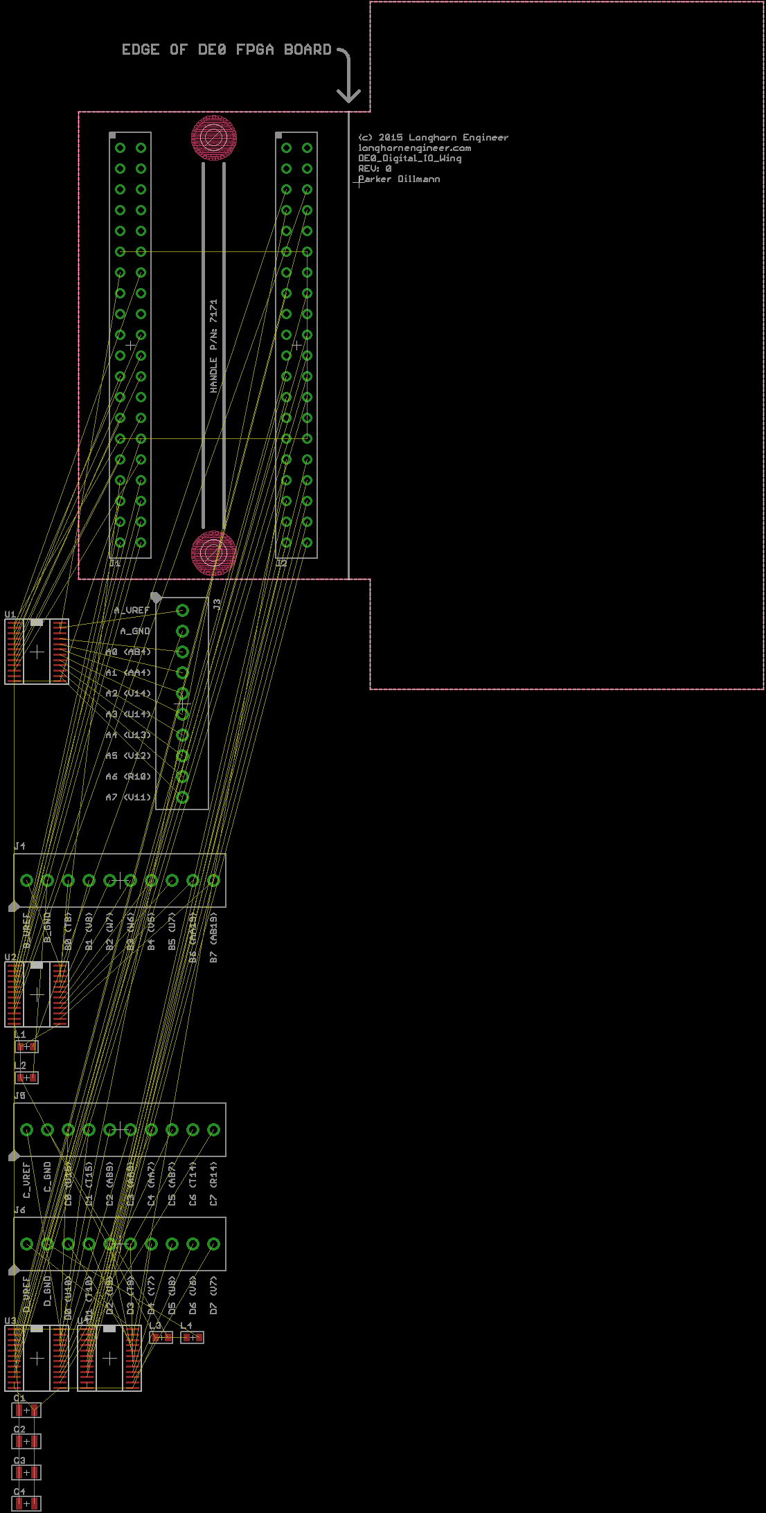
Started work on a expansion board for the DE0 FPGA development board. Planning on having 4 8-bit bi-directional level shifters giving 32 I/O and breaking out 12 LVDS signals to screw terminals. Basically a simple digital acquisition add on. Using the expansion template I made for the DE0 a couple days ago.
LVDS will be buffered to protect the FPGA. Have not picked the buffer chip yet. The bi-directional level shifter is the SN74LVC8T245PWR by Ti. Handles 1.65V to 5.5V on both sides and has basic ESD protection. I am debating putting over voltage protection on the I/O of the level shifters. A 50ohm resistor in series with the I/O plus a 5.6V TVS Diode should do the trick and not add to much cost to the board.
Uploaded the template that I use for making hardware expansions for the DE0 FPGA Dev board. It fits on the 2 40Pin GPIO Headers on the right side of the board. Files are for Eagle V6.0+
Here is the Booster Pack built. Tested and it works! I will be posting the code tomorrow after I clean it up some. Includes PWM for both channels and encoders (untested however). I will release a version with and without the encoders.