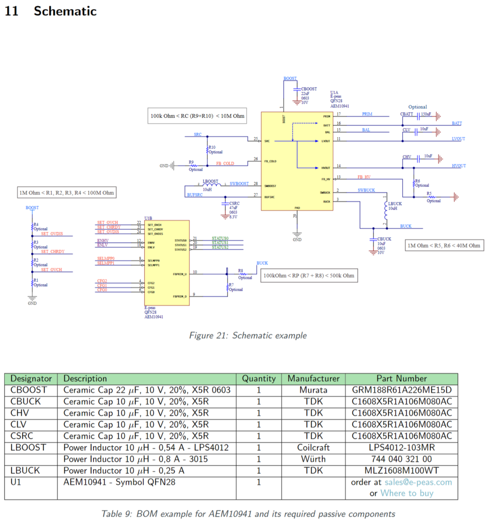
For the Cat Feeder Unreminder, the AEM10941 “ambient energy manager” has built in boost and buck regulators. These need external components like capacitors and inductors to function.
The example schematic in the datasheet for the AEM10941 looks like this and has these recommended components.
The capacitors are just your standard 0603, which are kinda small for the values. My project can handle larger sizes which will net better performance and lower leakage current.
For example GRM32ER61A106KA01L (10uF 10V X5R 1210) vs GRM155R61A106ME11 (10uF 10V X5R 0402). While its hard to specify leakage current as it varies with voltage, temperature, and frequency you can look at the insulation resistance and the larger the package the larger the insulation resistance.
Anyways, enough about capacitors. The Coilcraft inductor the schematic specs is from the LPS4012 series. I didn’t have this family in my EDA tool already designed so I opened up the datasheet to this horror.
This doesn’t look too bad but this showcases one of my pet peeves about how part manufactures dimension parts. Its pretty clear that mechanical engineers dimension parts. PCB Design tools don’t dimension like Mechanical Design Tools. In PCB tools, you typically specify the absolute location of the point/vertex of the line. This is different then Mechanical Design tools where you specify lengths and relationships between points.
For example look at this point right here that I circled in red.
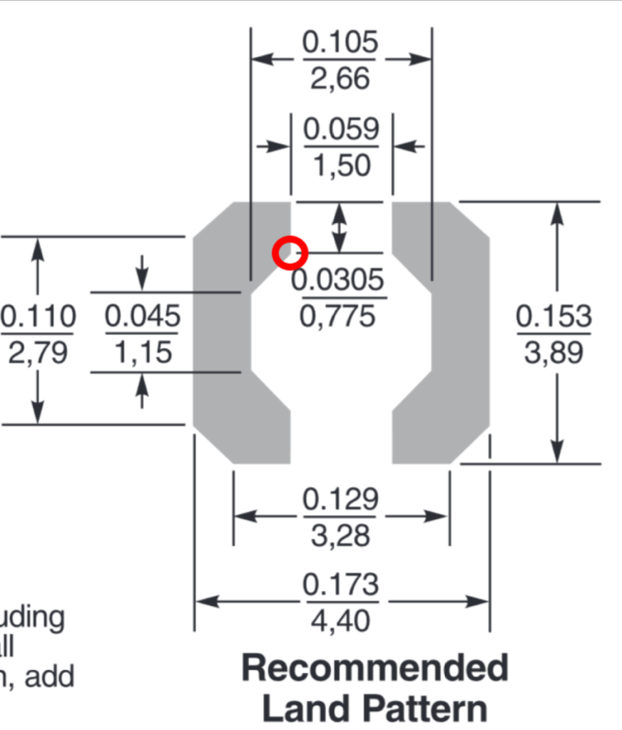
For the EDA tool I use (Eagle) the only way to do this is to tell that point of that polygon is at point (-0.75mm, 1.17mm) assuming the center of the part is (0, 0). X is easy, 1.5mm / 2. Y on the other hand is (3.89mm/2) – 0.775mm. Again just some arithmetic, but this is where the problems occur on validating new footprints and having to spin a prototype again just due to a slip of math.
Part manufacturers either need to give the data in a way that makes it easy to translate into the tools the electrical engineer uses or EDA tools need to become more like Mechanical tools in how you parametrically associate line edges and dimension footprints.
Now, I know that Autodesk has been working on bringing PCB layout design (and maybe schematic?) to the Fusion 360 ecosystem which would solve this problem. I don’t know how far along that product is but I should look into it for the next board I design. If Eagle libraries can be ported over then that would be rad.
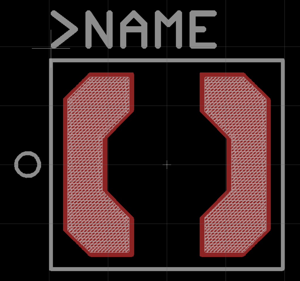
Anyways there is the part designed in Eagle. You can get it in my part library which is on github.