Its a small electronic device that makes sure you don’t overfeed your cat by feeding more often then needed. Low power consumption with no need of changing batteries or external power sources. Solar power? Basically a resettable egg timer that doesn’t need batteries cause if the batteries die then you won’t be reminded to feed the cat!
User interface should be simple. One button to reset the timer, then a LED that lights up when you are ok to feed the beasties and another LED that lets you know the system is working correctly. Maybe one led that is turned on when its not time to feed and then turns off when time to feed. Pressing the button resets and turns the LED back on? Verifying the circuit is still powered? Prevents hungry cats at least.
Simple BOM so far:
AEM10941
This is a Solar Energy Harvesting IC
DSF505Q6R0JBG
Super Caps
5F Capacitance!
Solar Panel AM-1816CA
84µA at peak power
This is specced at 200lx
LTC2956
Low power, configurable timer
Napkin math on power requirements. The LTC2956 draws 0.8μA. LED at 40uA. Total draw when Cat Feed Indicator is on is 40.8μA.
5F x (4.5V-3.6V) / 0.0000608 = 74,013 seconds -> 20 and a half hours!
So we have enough power from the fully charged Super Cap to run everything for almost a day. That is good. Should bump up the capacitance just to get a full day.
This is something I recorded with Stephen Kraig (Co-host of the MacroFab Engineering Podcast) back in September 2016. We never made it public till now! Drunken Gaming Night! It is silly and I have no idea where Stephen and I will take the channel but it is fun to do.
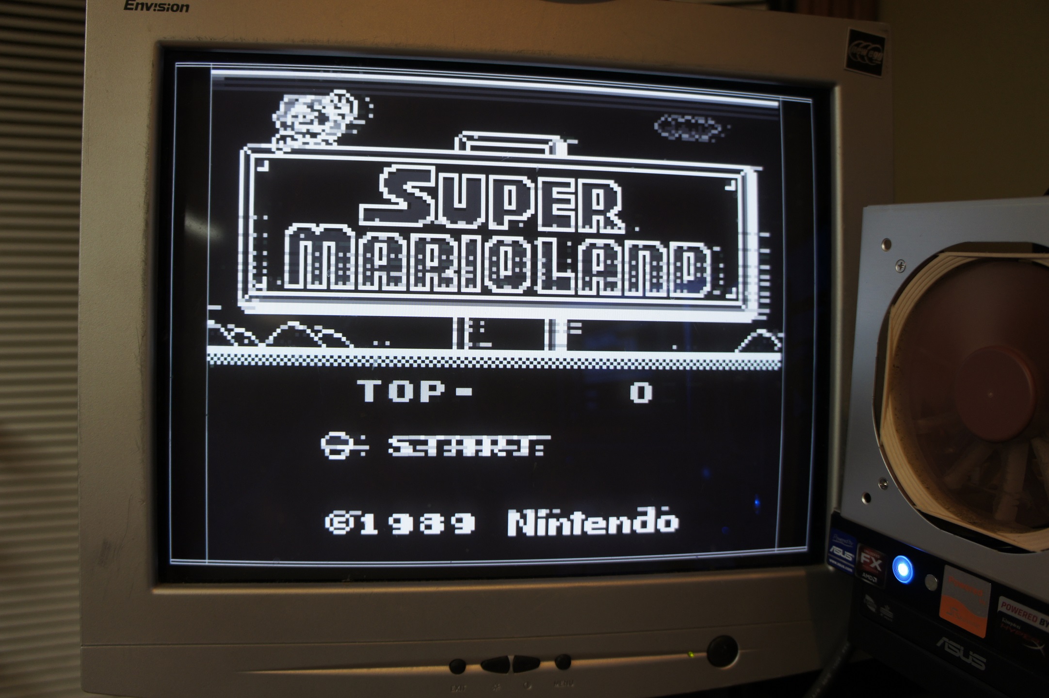
The DMG-01 Gameboy runs off all 5V logic and the FPGA I will be using (Cyclone 4 Altera) runs off 3.3V I/O. Conversion is needed to prevent frying the FPGA. I have used the TI part SN74LVC8T245 in the past with other FPGA projects and on the proof of concept VGA mod with the DE0 dev board.
The SN74LVC8T245’s output enable is active low so I pulled it high with a 10K resistor. This way the convertor is disabled till the FPGA can control the IC. Direction is set by default to be 5V -> 3.3V conversion with a 10K pull down.
I am also going to pull in the state of the buttons on the Gameboy. I hope to be able to have different modes that the FPGA can perform. Resolution changes and the like. Eventually I will design it so that FPGA can also drive the screen but that will probably be a future hardware revision.
Instead of trying to have an excuse of why I have not been posting here. Well go check out MacroFab. It is the company I co-founded a bit over 4 years ago now. I also am the co-host of the MEP or MacroFab Engineering Podcast. It is a weekly electronics podcast and we are currently on episode 119…and we have not missed a single week!
I have been doing side projects for fun but I have just been very bad about posting them here. Typically they just go to my twitter account and I talk about them on the podcast. I will be putting more effort into posting here.
With that out of the way… Current plan is to just look at my past incomplete projects and either finish them or kill them off. Starting with the FPGA Gameboy project. First order of business is to start making some dedicated hardware for the Gameboy. To quicken the development process I am going to lift the FPGA design block from the ChromaColor project. The FPGA is an older Cyclone 4 module (EP4CE6E22C8N) but it should do the trick and is still fairly affordable. I would like to move it to a newer platform like a 10M08SCU169C8G.
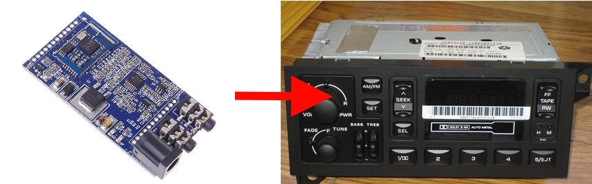
I have been working on my old 1999 TJ Jeep and I always wanted to have Bluetooth connectivity in for the stereo. I could have bought an after market head unit but I never really liked the look of them and they tend to be easily stolen out of the Jeep (softtop!). The stock head unit matches the dash and is less likely to be taken. Thus the solution was to hack in a Bluetooth module into the radio!
First I bought a used radio on ebay. Part number for the radio was P56038933AB and I was able to pick one up for $25 as I wanted to keep my radio functional in the Jeep till I got the Bluetooth working. Then I picked this module on amazon. I chose this module as it had a wide input voltage, every single connection and signal was brought out to a header, and it had good reviews.
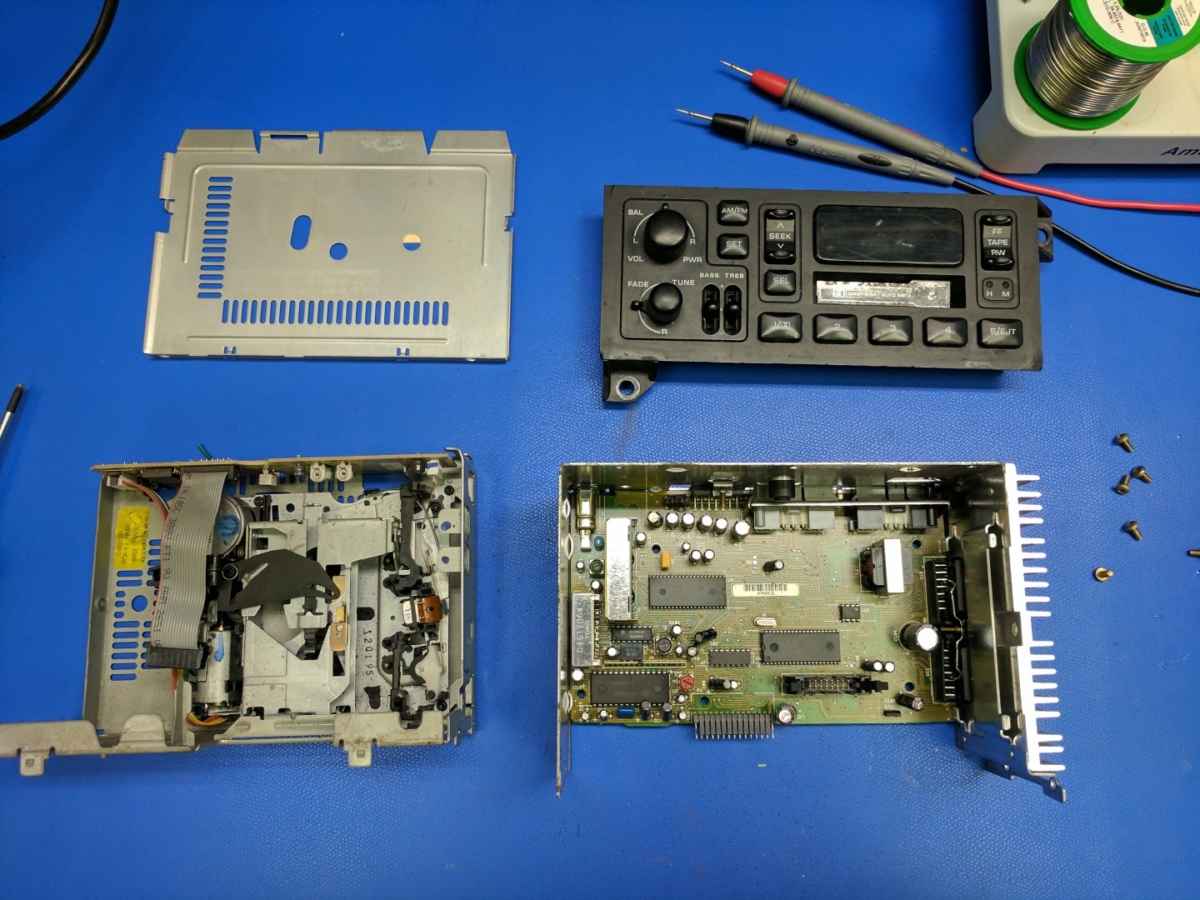
Next I opened the radio. It had T15 Torx (jeep thing :| ) machine screws that held it all together. Took it apart all the way to the bare radio.
Next to figure out how to get the Bluetooth signal injected into the radio! Most people that do these kind of hacks just blindly poke around the radio till they find and audio signal and then inject there. This is fine but I wanted to make sure I was getting the best audio quality out of my cheap Bluetooth module and early 90’s designed, base model head unit. I also wanted to keep the volume knob on the radio functional. This meant injecting the Bluetooth signal in the circuit before the power amplifiers and before it was gained for volume.
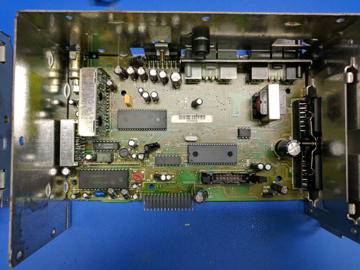
To figure out where to inject the audio. I first wrote down all the IC Manufactures, Part numbers, and Package size. Clicking the links will show an image of the IC.
Next I started searching for stuff like “ST Audio DIP42” into google. After finding promising datasheets, I then verified their pinouts buy tracing the power and ground sources in the radio. Here is the cross reference of what I was able to find. I also found this interesting PDF which is a early 90’s listing for ST Micro parts. I was able to find the TDA7340S IC with it.
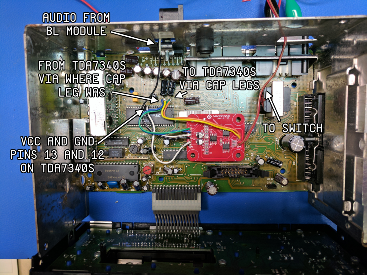
The IC that does the sound muxing, volume, and tone control is the TDA7340S and I figured this would be the best place to inject the Bluetooth audio signal.
Above is the block diagram. After the audio mux the signal travels to an external effects loop which consists of in series 1uF electrolytic capacitors. Then the audio signal travels into the volume and tone control parts. Perfect! If I inject the audio right before the capacitors I will retain the volume and tone control of the radio.
I thought about using the unused PHONE IN and then using a MCU to sniff the I2C buss and inject the right commands to switch it to that input but figured that would be more work then just injecting in the effects loop.
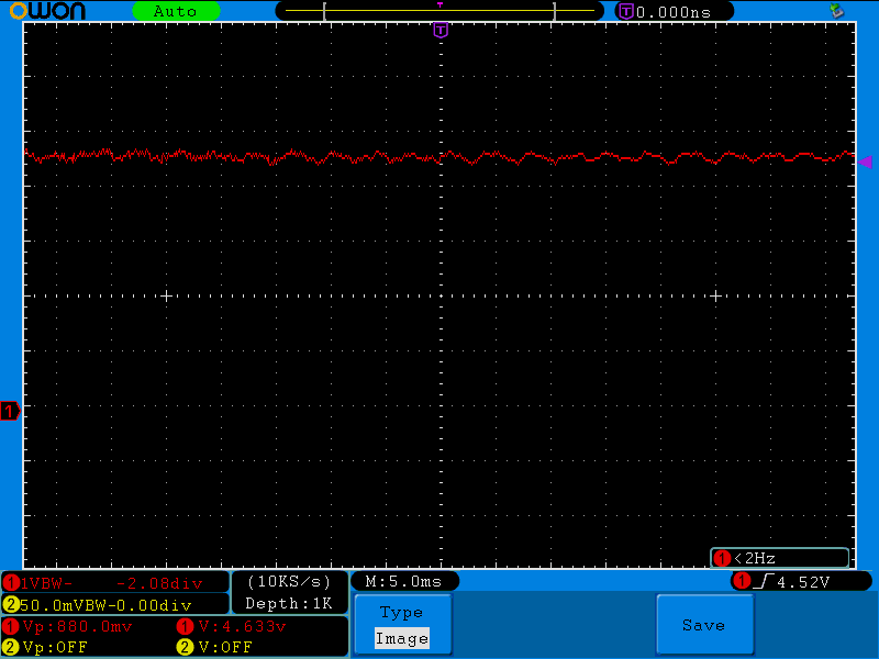
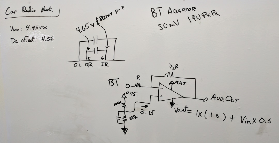
The next part is to make sure the signal from the Bluetooth adapter is compatible with what the TDA7340S is expecting. At max volume on my phone the Bluetooth adapter outputs a ~50mV DC offset signal with a ~1.7V to ~1.9V Pk-Pk. The signal in the effects loop was 4.65V DC offset signal with a 800mV Pk-Pk.
Bluetooth Module output at max volume.
Output of the TDA7340S effects loop. This would need to be matched to ensure compatibility.
Since these signals are different I needed to adjust the signal of the Bluetooth adapter. I would need to apply a DC offset and then negative gain the signal from the Bluetooth signal. The opamp circuit below should do the trick. The feedback circuit is set to half gain and by applying half of VCC (via a voltage divider) to the other input of the opamp we can DC offset the signal.
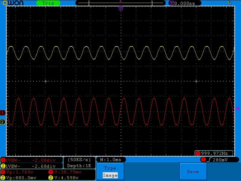
I tested it by having my phone play a tone via a tone generator app called “Frequency Sound Generator”. Signal below.
The input is in red and the output is in yellow. Signal now matches closely to what the TDA7340S expects their to be in the effects loop!
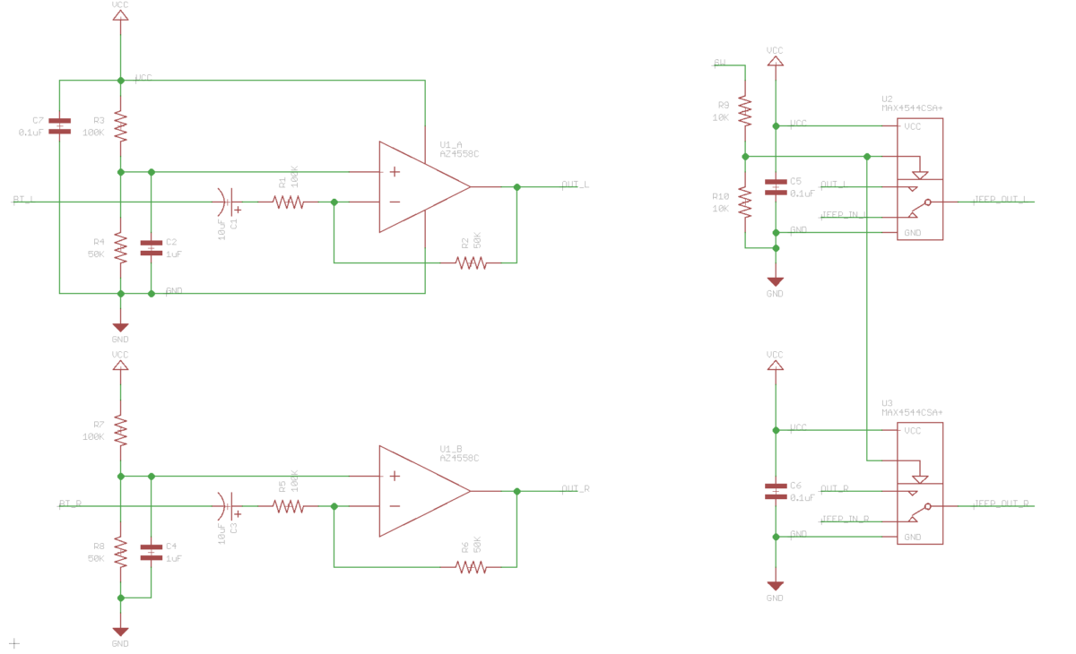
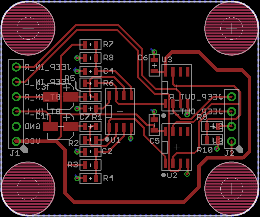
Then to switch between the TDA7340S signal and the Bluetooth signal I found an analog switch IC made by Maxim, MAX4544CSA+. The opamp I decided to use was a AZ4558C. I decided to use it because it is a decent audio amp and fairly inexpensive. Lastly, since its stereo we need to double everything. Below is the schematic and layout I did in Eagle.
The files for the board can be found on my github. I uploaded the files to MacroFab and ordered the board.
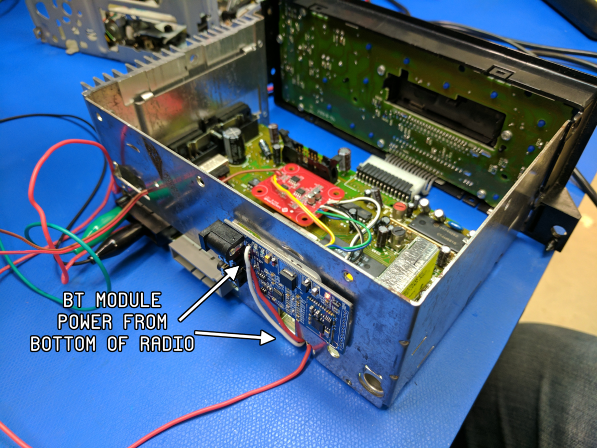
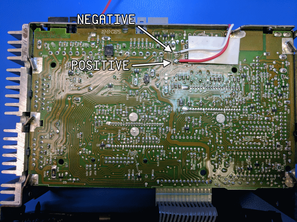
I then soldered the board into the radio. I desoldered one leg of the the effects loop 1uF caps which are designators C112 and C113, then soldered hook up wire on the legs of the capacitors and into the hole in the PCB. The power for the Bluetooth module is pulled from the bottom of the radio. To switch the audio from the TDA7340S to the Bluetooth the input of the MAX4544CSA+ is pulled up. A switch on the dash will be used for this. See image below for how everything is hooked up.
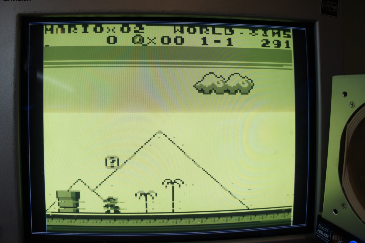
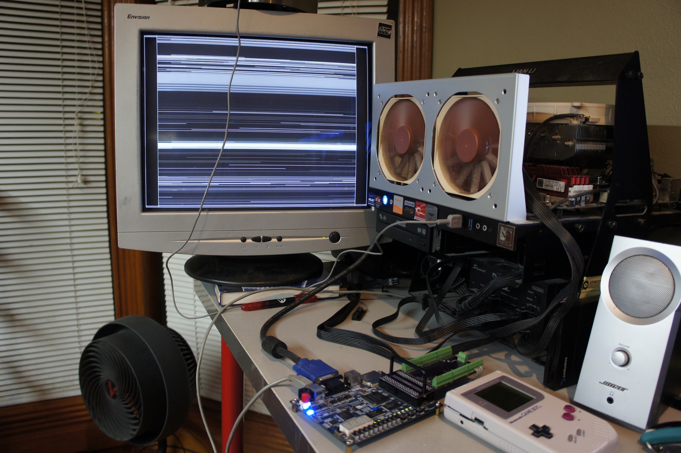
I have some seemingly random video glitches to iron out but it is much better then previously. I will probably need to recode my capture routine as a state engine to make further advancements.
Currently the Gameboy LCD sniffer verilog code is just pulling data from the LCD bus without worrying about the clocks and putting it into the display ram. Basically just testing the level shifters. They work! Should be able to bang out the rest of the code tomorrow.
This is the project that the DE0 Digital IO Wing is for. I will use the IO wing to level shift the signals from the Gameboy’s LCD screen so my DE0 can capture the data. The Gameboy is a 5V device and the DE0 does not have 5V tolerant IO. I am using a SN74LVC8T245PWR 8-bit directional level shifter to do the translation on the IO wing board.
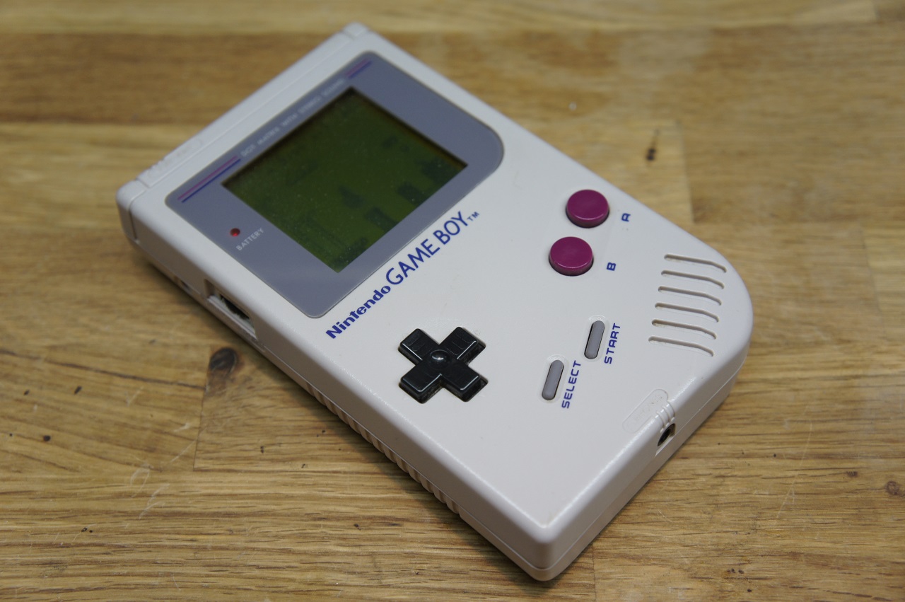
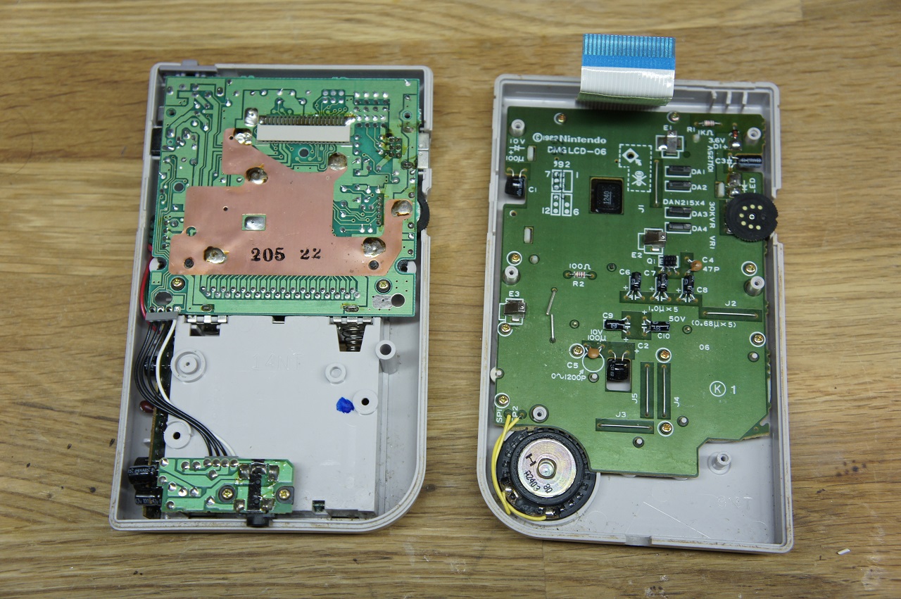
Gameboy DMG-01.
Purchased a Gameboy DMG-01 off eBay for $20. Needed some cleaning but it worked and had the battery cover!
Taking apart the Gameboy DMG-01.
The Gameboy DMG-01 uses triwing screws. Kidna like philips heads but with 3 “wings” instead of 4. Tool can be found on eBay or Amazon.
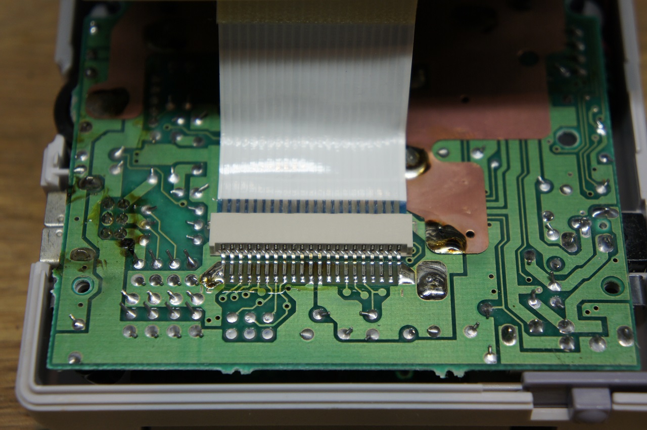
Front board and LCD connector for the Gameboy DMG-01.
The connector between the front and back of the Gameboy is where I will tap into the signals to sneak a peak. Pinout is the following
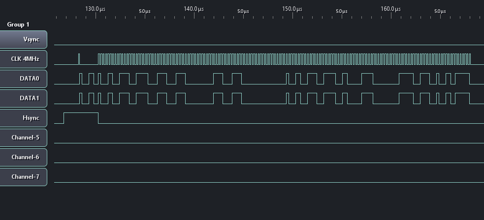
V-Sync should be 60Hz, Pixel Clock 4Mhz, and H-Sync 9.2kHz.
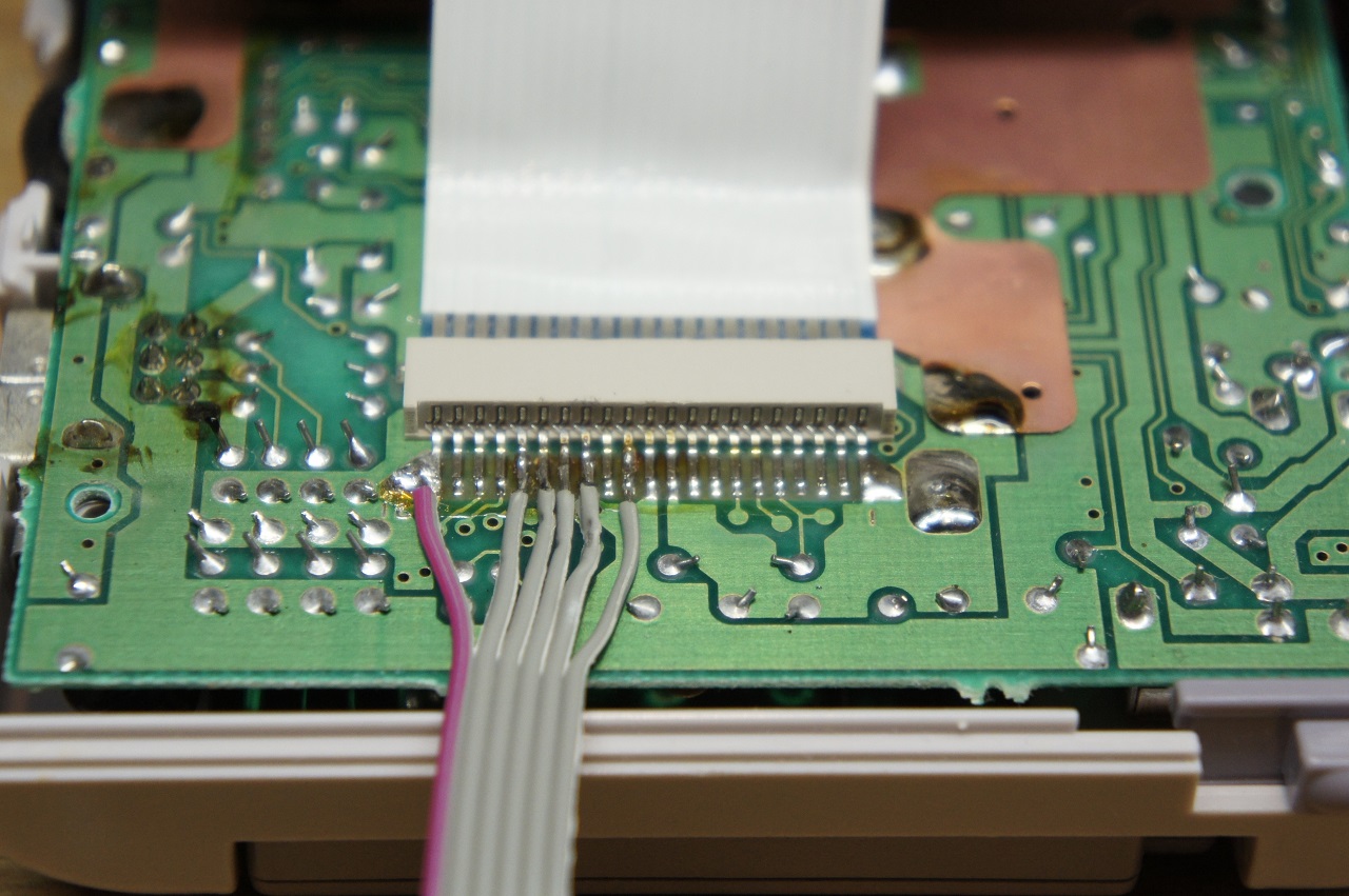
Wires to sniff the connector.
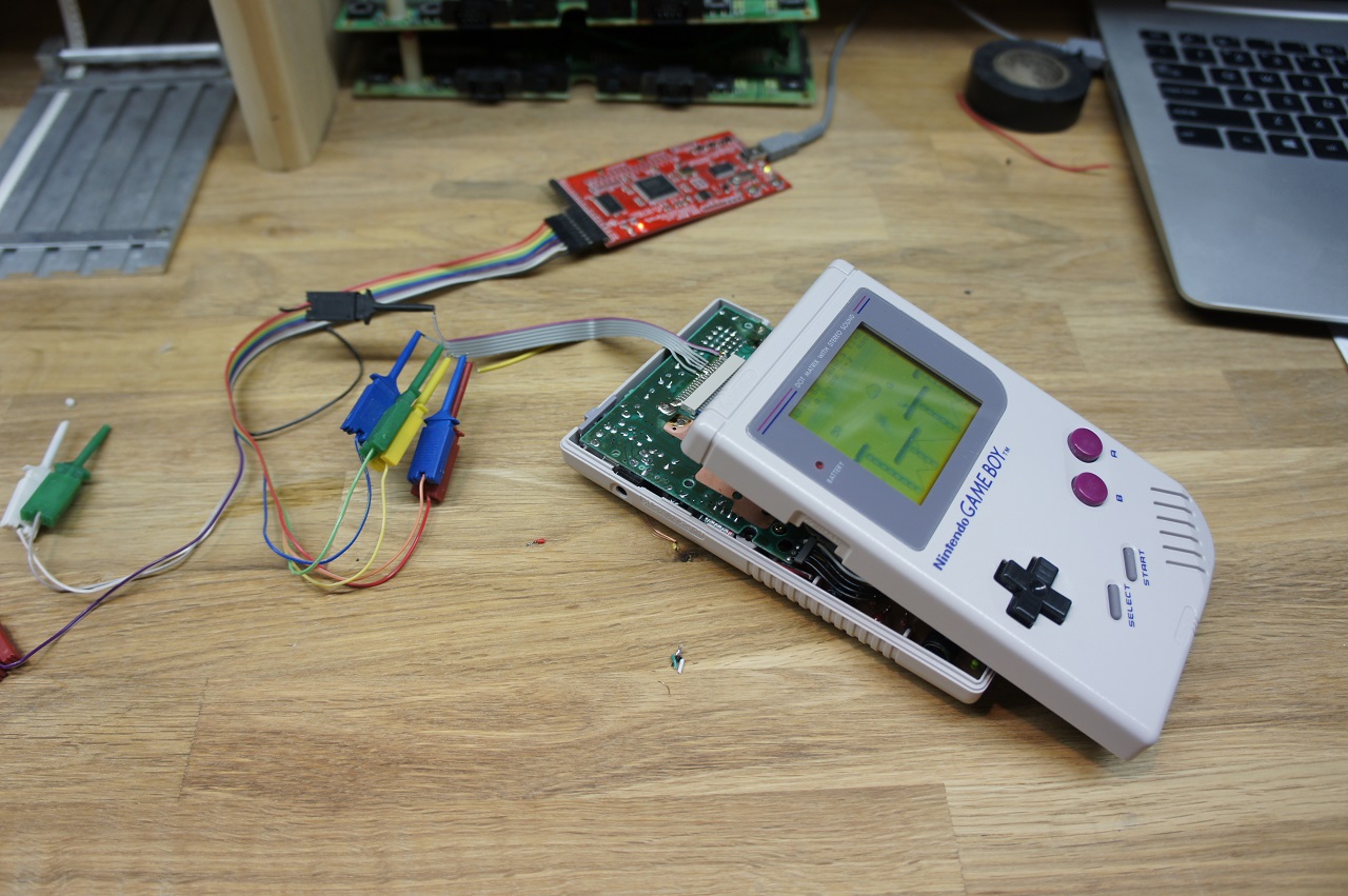
Open Bench Logic Sniffer connected to Gameboy DMG-01.
Connected up the Open Bench Logic Sniffer and powered up the Gameboy with a game in it then ran the capture. I had the trigger set to wait for the V-Sync signal.
Entire V-Sync frame. Hard to see much detail.
Frame zoomed in a bit to see the individual horizontal lines.
Complete horizontal frame.
Then using my DE0_VGA_Driver I started writing the code take data from RAM on the FPGA and output it on the VGA monitor. I wrote a bitmap to .mif format (memory initialization file) convertor to display some Gameboy screenshots on the VGA Monitor. Link to that repo is here.
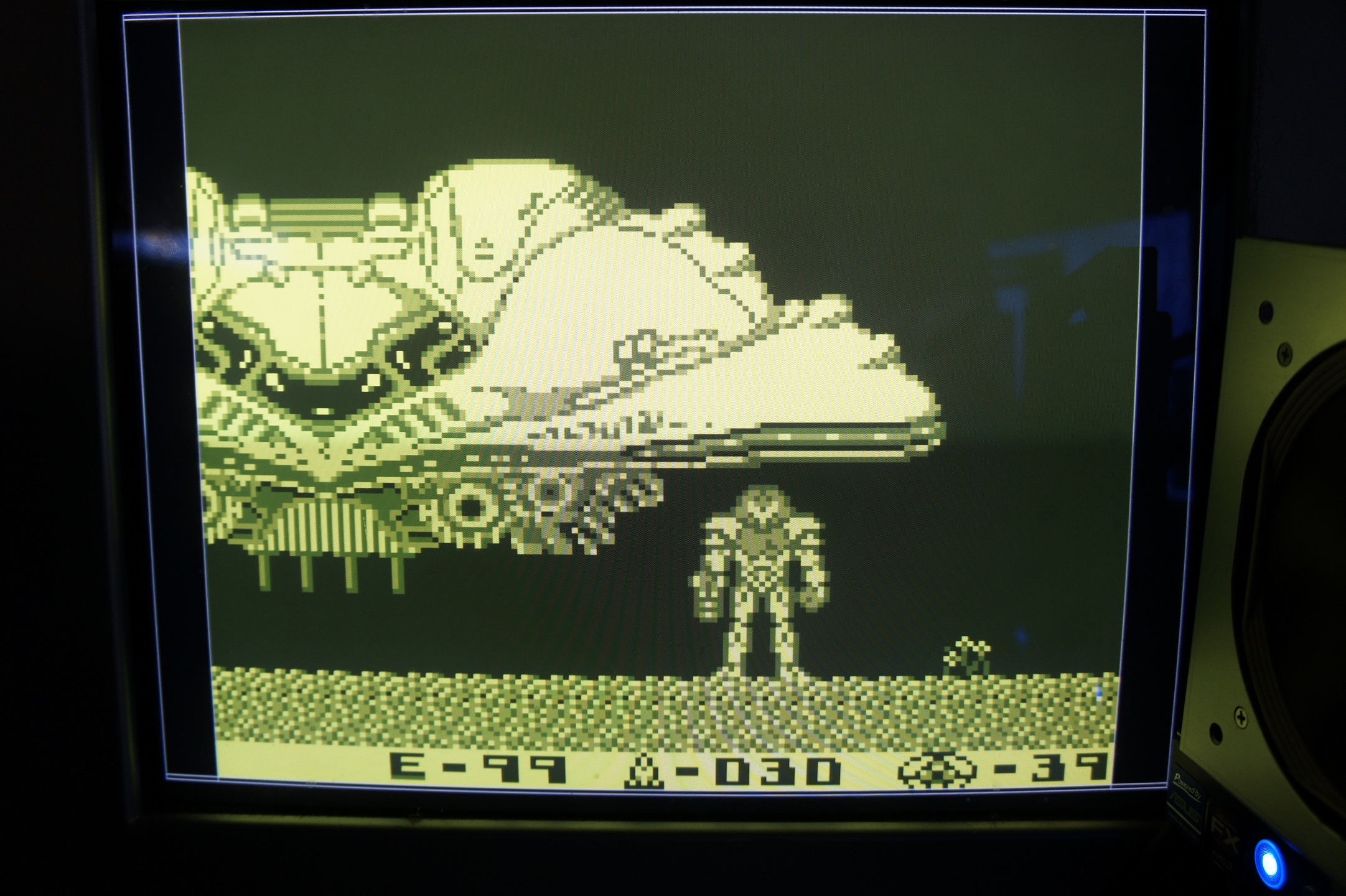
Gameboy DMG-01 screenshot displayed from DE0 FPGA RAM. Simulating original Gameboy “yellow-green” pallet.
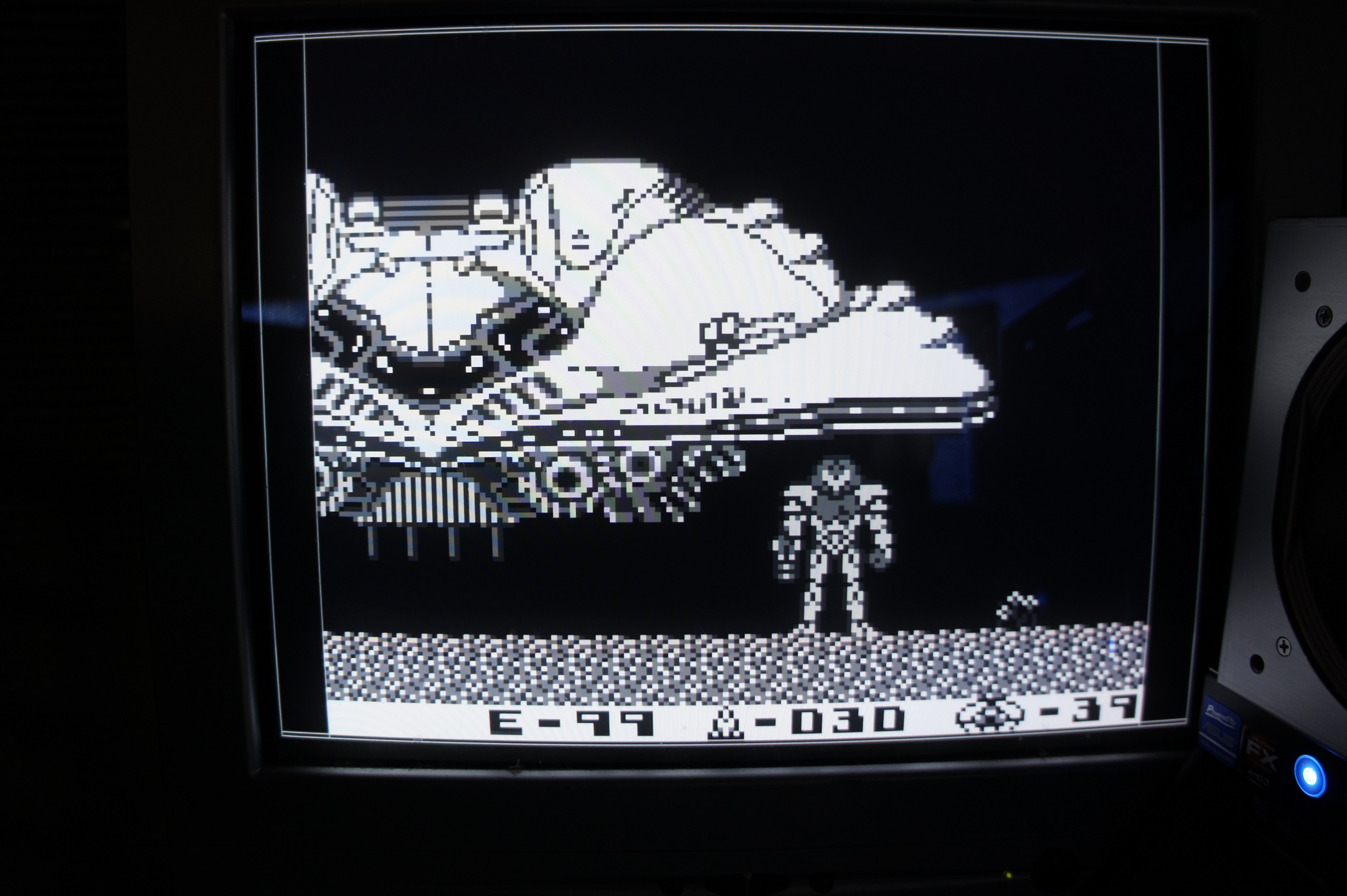
Gameboy DMG-01 screenshot displayed from DE0 FPGA RAM. Using B/W color scheme.
Currently working on getting the SN74LVC8T245PWR level shifters working and I will be able to pull live data from the Gameboy LCD data bus.