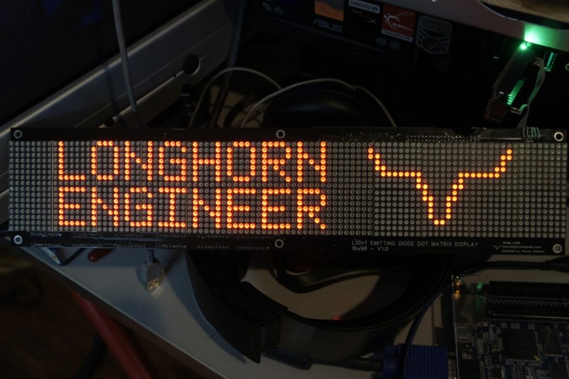
Fixed an old bug in some RESET VECTOR DMD display code for multiple lines and got the above demo working. I will have to port the prop code to python however to make my twitter wall thingy.
Tag Archives: RESET_VECTOR
16×96 DMD Code for Reset Vector
While developing the larger 36×128 DMD I ran out of registers and logic elements in the FPGA I was using. I could have switched to a larger FPGA but that would put the final product out of the price range I was aiming for. FPGAs have loads of dedicated ram so I decided to move the display memory from registers to a chunk of block ram. To test to see if the RAM code works I wrote a program for the 16×96 display in RESET_VECTOR. It took a bit of tweaking as I have never used block ram before but I was able to get it working.
module LED_Matrix_16x96
(
clk,row,col,SDRAM_CS,SRAM_CS,LAT,INPUT,SCLK
);
input wire clk;
input wire LAT;
input wire INPUT;
input wire SCLK;
output reg [0:15] row;
output reg [95:0] col;
output reg [0:0] SDRAM_CS;
output reg [0:0] SRAM_CS;
reg [24:0] clk_slow;
reg [4:0] row_cnt;
reg [1535:0] col_buffer;
reg [3:0] read_addr;
reg [3:0] write_addr;
reg [95:0] disp_mem_data;
reg disp_mem_wren;
wire [95:0] disp_mem_q;
reg [3:0] sel;
initial
begin
row <= 16'b0000000000000001;
    col <= 16'b0000000000000000;
    SDRAM_CS <= 1'b0;
    SRAM_CS <= 1'b0;
    clk_slow <= 16'b0000000000000000;
    row_cnt <= 5'b00000;
    write_addr <= 4'b0000;
    read_addr <= 4'b0000;
    disp_mem_wren <= 0;
    sel <= 4'b0000;
  end

always @(posedge clk)
begin
  clk_slow <= clk_slow + 1'b1;

  if(!LAT & row_cnt == 5'b01111)
  begin
  case(sel)
    4'b0000:
    begin
      write_addr <= sel;
      disp_mem_wren <= 1'b1;
      disp_mem_data <= col_buffer[1535:1440];
      sel <= 4'b0001;
    end
    4'b0001:
    begin
      write_addr <= sel;
      disp_mem_wren <= 1'b1;
      disp_mem_data <= col_buffer[1439:1344];
      sel <= 4'b0010;
    end
    4'b0010:
    begin
      write_addr <= sel;
      disp_mem_wren <= 1'b1;
      disp_mem_data <= col_buffer[1343:1248];
      sel <= 4'b0011;
    end
    4'b0011:
    begin
      write_addr <= sel;
      disp_mem_wren <= 1'b1;
      disp_mem_data <= col_buffer[1247:1152];
      sel <= 4'b0100;
    end
    4'b0100:
    begin
      write_addr <= sel;
      disp_mem_wren <= 1'b1;
      disp_mem_data <= col_buffer[1151:1056];
      sel <= 4'b0101;
    end
    4'b0101:
    begin
      write_addr <= sel;
      disp_mem_wren <= 1'b1;
      disp_mem_data <= col_buffer[1055:960];
      sel <= 4'b0110;
    end
    4'b0110:
    begin
      write_addr <= sel;
      disp_mem_wren <= 1'b1;
      disp_mem_data <= col_buffer[959:864];
      sel <= 4'b0111;
    end
    4'b0111:
    begin
      write_addr <= sel;
      disp_mem_wren <= 1'b1;
      disp_mem_data <= col_buffer[863:768];
      sel <= 4'b1000;
    end
    4'b1000:
    begin
      write_addr <= sel;
      disp_mem_wren <= 1'b1;
      disp_mem_data <= col_buffer[767:672];
      sel <= 4'b1001;
    end
    4'b1001:
    begin
      write_addr <= sel;
      disp_mem_wren <= 1'b1;
      disp_mem_data <= col_buffer[671:576];
      sel <= 4'b1010;
    end
    4'b1010:
    begin
      write_addr <= sel;
      disp_mem_wren <= 1'b1;
      disp_mem_data <= col_buffer[575:480];
      sel <= 4'b1011;
    end
    4'b1011:
    begin
      write_addr <= sel;
      disp_mem_wren <= 1'b1;
      disp_mem_data <= col_buffer[479:384];
      sel <= 4'b1100;
    end
    4'b1100:
    begin
      write_addr <= sel;
      disp_mem_wren <= 1'b1;
      disp_mem_data <= col_buffer[383:288];
      sel <= 4'b1101;
    end
    4'b1101:
    begin
      write_addr <= sel;
      disp_mem_wren <= 1'b1;
      disp_mem_data <= col_buffer[287:192];
      sel <= 4'b1110;
    end
    4'b1110:
    begin
      write_addr <= sel;
      disp_mem_wren <= 1'b1;
      disp_mem_data <= col_buffer[191:96];
      sel <= 4'b1111;
    end
    4'b1111:
    begin
      write_addr <= sel;
      disp_mem_wren <= 1'b1;
      disp_mem_data <= col_buffer[95:0];
      sel <= 4'b0000;
    end
    default:
    begin
      sel <= 4'b0000;
      write_addr <= 4'b0000;
      disp_mem_wren <= 1'b0;
    end
  endcase
  end
  else
  begin
    disp_mem_wren <= 1'b0;
    sel <= 4'b0000;
  end
end

always @(posedge clk_slow[10])
begin
  if(row_cnt > 5'b01111)
begin
row_cnt <= 5'b00000;
  end
  col <= disp_mem_q;
  row_cnt <= row_cnt + 1'b1;
  row <= {row[15],row[0:14]};
  read_addr <= read_addr + 1'b1;

end

always @(posedge SCLK)
begin
  if(LAT)
  begin
    col_buffer <= {col_buffer[1534:0],INPUT};
  end
end

display_ram disp_mem_inst (
        .rdaddress (read_addr),
        .wraddress (write_addr),
        .clock  (clk),
        .data   (disp_mem_data),
        .wren   (disp_mem_wren),
        .q      (disp_mem_q)
);

endmodule
LDMD 16×16 Propeller Comm Test
Just finished the DMD (Dot Matrix Display) test for RESET_VECTOR. Since the Propeller is to slow to do the matrixing I am going to use a FPGA to do it. The propeller will send the data over a serial connection into a frame buffer on the FPGA. When all the data is on the FPGA the FPGA will update its matrixing buffer.
I have the Propeller to FPGA communication protocol written and tested as well. The Propeller loads the Data off the SD card and sends it serially to the FPGA.
Propeller Code
FPGA Code
Block Diagram of the Dot Matrix.


