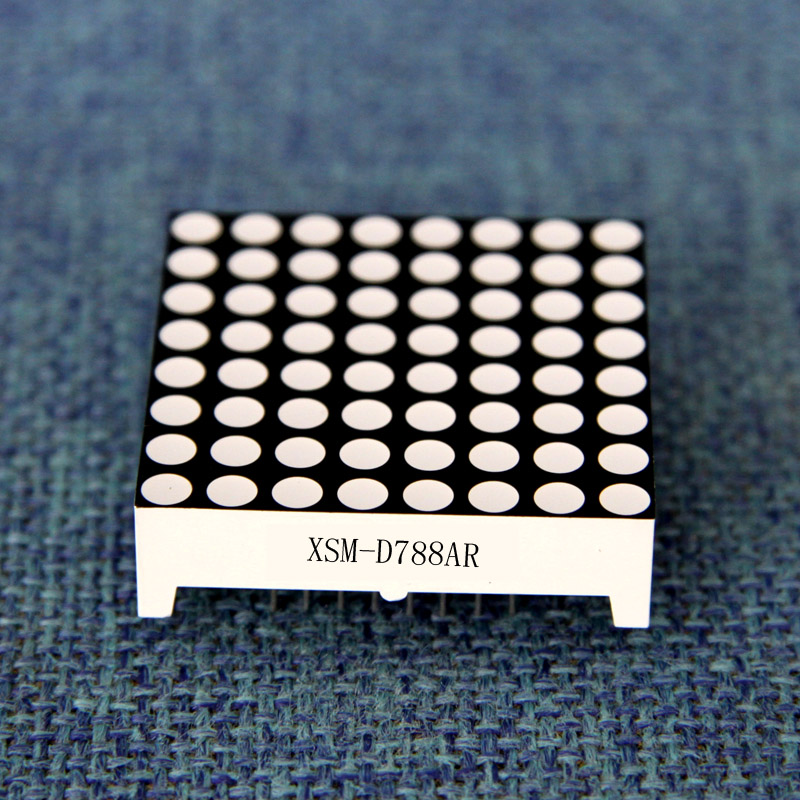
8×8 LED Matrix Modules in 1.9mm size

So for the new 128×32 DMD I am using a smaller dot pitch LED Matrix with a size of 1.9mm. This means they are the same size as standard DMDs used on production machines. I secured a supplier and I can provide any color LED for the DMDs. Red, Orange, Amber, Blue, Green, ect. These are currently not compatible with production machines but are intended for Home Brew Pinball machines. They are very easy to work with.

Instead of the wacky voltages of a standard DMD mine only needs a +5V supply. Standard DMDs also are hard to drive with microcontrollers because you have to fill each “level” individually and you have to do it fast enough to keep up with the refresh rate. My DMD runs off a FPGA which means you don’t have to worry about how fast you send the data to the display. The FPGA takes care of all the matrixing and color levels. All you have to do is send the data in 1byte wide chunks which is perfect for Microcontroller use. If you are doing animations you can stream data off an SD card by doing byte writes and then pushing that data directly to the DMD.

Prices will be $250 for quantities 1-9 and $240 for anything over 10. They come with the SMD parts soldered on and the FPGA pre-programmed. You will need to solder the LED modules on. The LED modules will be tested to ensure that they are in full working order.

Code tweaking on Reset_Vector

So I was still getting glitches on my inputs for Reset_Vector. I couldn’t figure out what was causing it because it would happen randomly and I couldn’t repeat the problem. The false inputs caused issues with ball triggering, score detection, and playfield actions. I figured it had to be glitches on the lines caused by EMF or something on the input driver. I knew it was the input driver cause when a solenoid fired randomly like the pop bumper it would register a hit which means that the microcontroller detected a hit.

To fix this issue I added a simple debouncer routine. Basically it makes sure a input is pressed for at least 2 Kernel cycles before saying that it was a hit. This keeps random spikes from registering as hits.

What it does is read in the inputs into a variable called new_inputs. The new_inputs then gets anded with a variable called old_inputs and the result is the inputs that where held for two kernel cycles. Then the new_inputs is copied into old_inputs for the next cycle to happen.

This system can be easily expanded to 3,4,ect cycles so the debouncer is extremely configurable in its sensitivity.

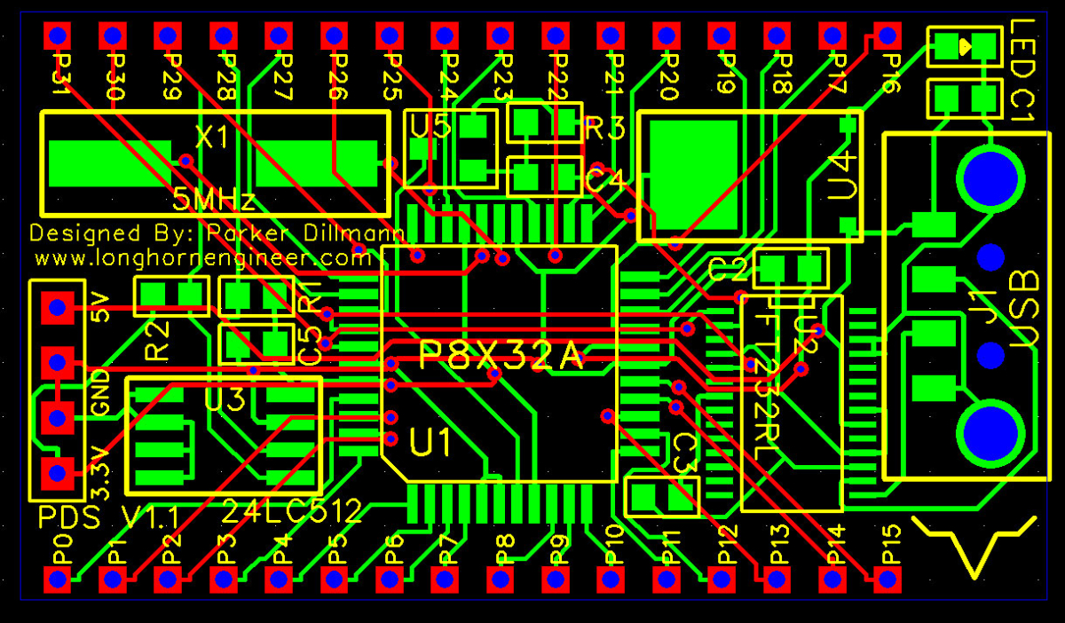
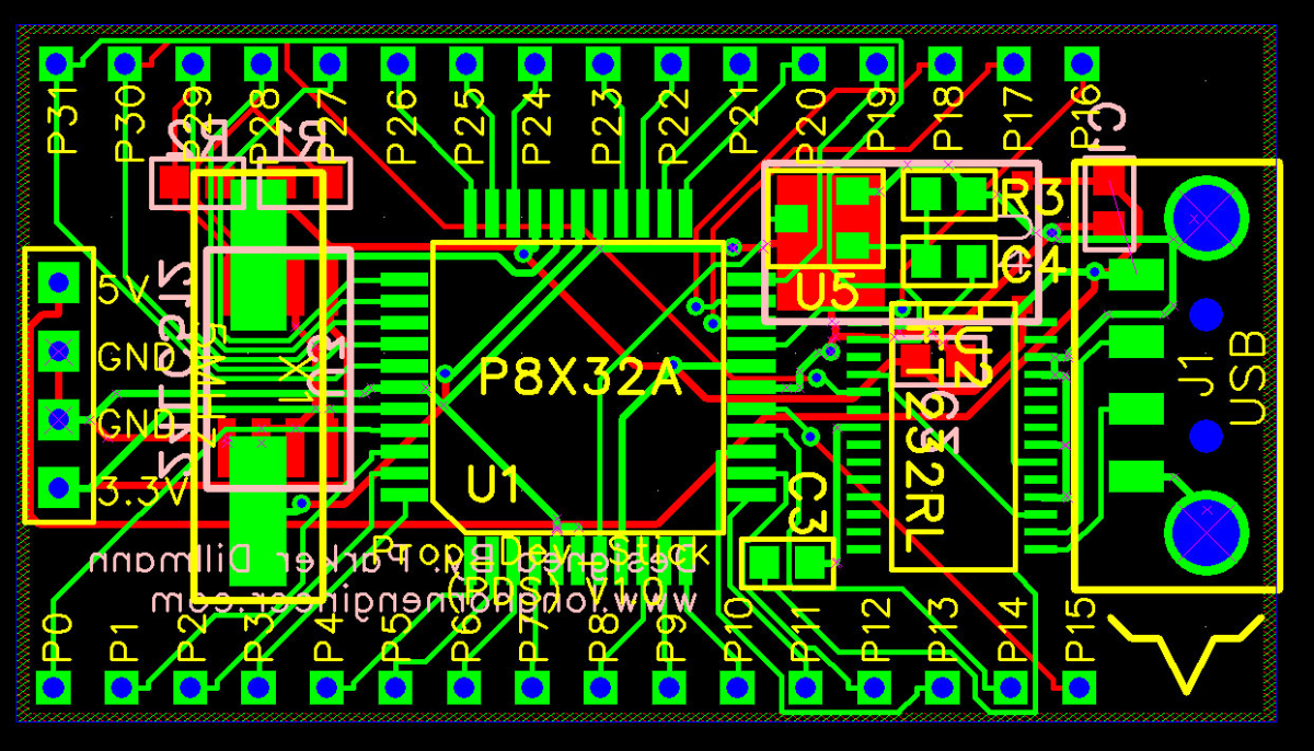
Late night PCB work.

I have had this idea to make a very small development board for the Propeller for a while now. The idea is that you can have it on your keychain or something and just plug the entire unit into a USB port. The port powers the device and there are female headers that allow you to plug other things into it. I might add a ADC just to get some analog signal input.

So I give you /drumroll the Propeller Development Stick or PDS V1.0.

16×96 DMD Code for Reset Vector

While developing the larger 36×128 DMD I ran out of registers and logic elements in the FPGA I was using. I could have switched to a larger FPGA but that would put the final product out of the price range I was aiming for. FPGAs have loads of dedicated ram so I decided to move the display memory from registers to a chunk of block ram. To test to see if the RAM code works I wrote a program for the 16×96 display in RESET_VECTOR. It took a bit of tweaking as I have never used block ram before but I was able to get it working.


module LED_Matrix_16x96
(
clk,row,col,SDRAM_CS,SRAM_CS,LAT,INPUT,SCLK
);

input  wire    clk;
input  wire    LAT;
input  wire    INPUT;
input  wire    SCLK;

output  reg [0:15]  row;
output  reg [95:0]  col;
output  reg [0:0]   SDRAM_CS;
output  reg [0:0]   SRAM_CS;

reg [24:0]  clk_slow;
reg [4:0]  row_cnt;
reg [1535:0]  col_buffer;

reg  [3:0]  read_addr;
reg  [3:0]  write_addr;
reg  [95:0]  disp_mem_data;
reg      disp_mem_wren;
wire  [95:0]  disp_mem_q;

reg [3:0]  sel;

initial
begin
row <= 16'b0000000000000001;
    col <= 16'b0000000000000000;
    SDRAM_CS <= 1'b0;
    SRAM_CS <= 1'b0;
    clk_slow <= 16'b0000000000000000;
    row_cnt <= 5'b00000;
    write_addr <= 4'b0000;
    read_addr <= 4'b0000;
    disp_mem_wren <= 0;
    sel <= 4'b0000;
  end

always @(posedge clk) 
begin
  clk_slow <= clk_slow + 1'b1;

  if(!LAT & row_cnt == 5'b01111)
  begin
  case(sel)
    4'b0000:
    begin
      write_addr <= sel;
      disp_mem_wren <= 1'b1;
      disp_mem_data <= col_buffer[1535:1440];
      sel <= 4'b0001;
    end
    4'b0001:
    begin
      write_addr <= sel;
      disp_mem_wren <= 1'b1;
      disp_mem_data <= col_buffer[1439:1344];
      sel <= 4'b0010;
    end    
    4'b0010:
    begin
      write_addr <= sel;
      disp_mem_wren <= 1'b1;
      disp_mem_data <= col_buffer[1343:1248];
      sel <= 4'b0011;
    end    
    4'b0011:
    begin
      write_addr <= sel;
      disp_mem_wren <= 1'b1;
      disp_mem_data <= col_buffer[1247:1152];
      sel <= 4'b0100;
    end    
    4'b0100:
    begin
      write_addr <= sel;
      disp_mem_wren <= 1'b1;
      disp_mem_data <= col_buffer[1151:1056];
      sel <= 4'b0101;
    end    
    4'b0101:
    begin
      write_addr <= sel;
      disp_mem_wren <= 1'b1;
      disp_mem_data <= col_buffer[1055:960];
      sel <= 4'b0110;
    end
    4'b0110:
    begin
      write_addr <= sel;
      disp_mem_wren <= 1'b1;
      disp_mem_data <= col_buffer[959:864];
      sel <= 4'b0111;
    end
    4'b0111:
    begin
      write_addr <= sel;
      disp_mem_wren <= 1'b1;
      disp_mem_data <= col_buffer[863:768];
      sel <= 4'b1000;
    end
    4'b1000:
    begin
      write_addr <= sel;
      disp_mem_wren <= 1'b1;
      disp_mem_data <= col_buffer[767:672];
      sel <= 4'b1001;
    end
    4'b1001:
    begin
      write_addr <= sel;
      disp_mem_wren <= 1'b1;
      disp_mem_data <= col_buffer[671:576];
      sel <= 4'b1010;
    end    
    4'b1010:
    begin
      write_addr <= sel;
      disp_mem_wren <= 1'b1;
      disp_mem_data <= col_buffer[575:480];
      sel <= 4'b1011;
    end
    4'b1011:
    begin
      write_addr <= sel;
      disp_mem_wren <= 1'b1;
      disp_mem_data <= col_buffer[479:384];
      sel <= 4'b1100;
    end
    4'b1100:
    begin
      write_addr <= sel;
      disp_mem_wren <= 1'b1;
      disp_mem_data <= col_buffer[383:288];
      sel <= 4'b1101;
    end
    4'b1101:
    begin
      write_addr <= sel;
      disp_mem_wren <= 1'b1;
      disp_mem_data <= col_buffer[287:192];
      sel <= 4'b1110;
    end
    4'b1110:
    begin
      write_addr <= sel;
      disp_mem_wren <= 1'b1;
      disp_mem_data <= col_buffer[191:96];
      sel <= 4'b1111;
    end
    4'b1111:
    begin
      write_addr <= sel;
      disp_mem_wren <= 1'b1;
      disp_mem_data <= col_buffer[95:0];
      sel <= 4'b0000;
    end
    default: 
    begin
      sel <= 4'b0000;
      write_addr <= 4'b0000;
      disp_mem_wren <= 1'b0;
    end
  endcase
  end
  else
  begin
    disp_mem_wren <= 1'b0;
    sel <= 4'b0000;
  end
end

always @(posedge clk_slow[10]) 
begin
  if(row_cnt > 5'b01111)
begin
row_cnt <= 5'b00000;
  end
  col <= disp_mem_q;  
  row_cnt <= row_cnt + 1'b1;
  row <= {row[15],row[0:14]};
  read_addr <= read_addr + 1'b1;

end

always @(posedge SCLK)
begin
  if(LAT)
  begin
    col_buffer <= {col_buffer[1534:0],INPUT};
  end
end

display_ram disp_mem_inst (
        .rdaddress (read_addr),
        .wraddress (write_addr),
        .clock  (clk),
        .data   (disp_mem_data),
        .wren   (disp_mem_wren),
        .q      (disp_mem_q)
);

endmodule

MSP-430: Servo and Accel demo Update

Awhile ago I uploaded a demo of the Fraunch Board that used the Accelerometer and outputted it to a set of servos. I made a video demonstrating it but I forgot to upload it.

http://www.youtube.com/watch?v=HttK_tMvNzM

The MSP-EXP430FR5739 board has a built in AXL335 which is a 3-axis accelerometer. It is hard wired to ports P3.0, P3.1, and P3.2. There was no demo code how to get the ADC10 to read those values.

I looked into the sequential sampling that the MSP430 supports which is where ADC10INCHx is set to the last ADC port and will go all the way down to ADC10INCH0 in sequence. This is a problem on the Fraunch Pad as the AXL335 outputs are wired to P3.0 – P3.2 which means when you set ADC10INCHx to ADC10INCH14 (P3.2) it will process more then half the pins as analog inputs!

Solution was to change the ADC10INCHx between sampling so the ADC process became round robin style. Here is the working code to sample all the axises on the Fraunch board. Also included is the “zero” calibration routines.

This code also contains a twin servo routine. The servos are connected to P1.4 and P1.5. When the X-axis moves the servo on P1.4 moves and when the Y-axis moves the servo on P1.5.

Code


main.c
FR_EXP.h

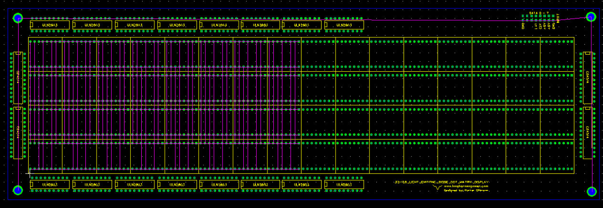
32×128 DMD Rat Lining Halfway Done

Halfway done with the rat lining for the PCB. A rat line is basically a visible line while PCB drawing that indicates net lists. A net list is just a list of all the pins and connections that are connected together. After I rat line I can lay down the traces.

The FPGA sees the display as a 64×64. This is due to I/O limitations. The odd rows are on the left and the even rows are on the right. So row 1 and 2 really make up the physical row 1.