Category Archives: PCBA & ENG

MSP-430 LaunchPad UART and FIFO

This code is currently for the MSP430G2553 on the Ti LaunchPad. The MSP430G2553 has a built in USCI that can be used for UART. Unlike lower end models of the value line you do not have to make a slow software UART. I looked online and did not see any UART libraries that where nice to work with without hacking them apart. I did not see any FIFO implementations at all either. They generally waited on the UART to finish its business before sending more data.

The advantage of the FIFO allows the MSP430 to push that data into the FIFO as fast as it can and let the hardware UART do the rest of the job. This frees up the CPU to do allot more stuff. The only bad thing is that if the FIFO gets full you start loosing data. The code has a global flag to let the main code know that the FIFOs are full.

The Receive (RX) portions of the code also have a global mailbox flag to notify the rest of the code that the UART received something. This would be useful if you need to send commands to a robot or device.

There are 4 different flavors of the code.

1. RX TX
2. RX TX with a FIFO
3. TX only
4. TX only with a FIFO

The code without the FIFOs waits on the UART during the transmission but uses far less memory then the FIFO code. You have to sacrifice speed or memory on this one. The TX only code strips out the RX portions if you just want to have the msp-430 print to a terminal. This is useful for debugging purposes.

If you are going to use this on the MSP-430 LaunchPad then you will need to cross the RX and TX lines. This pdf I found on the internet explains on page 3 (step 6) what I am talking about.

RX TX UART Code (CCS V5)
Project File
main.c
uart.c
uart.h

RX TX UART FIFO Code (CCS V5)
Project File
main.c
uart_fifo.c
uart_fifo.h

TX UART Code (CCS V5)
Project File
main.c
uart_tx.c
uart_tx.h

TX UART FIFO Code (CCS V5)
Project File
main.c
uart_fifo_tx.c
uart_fifo_tx.h

FIFO Code (CCS V5)
Project File
fifo_.c
fifo.h

Super Boost

This is the how to page on how to build the SUPER BOOST pcb. Please refer to the disclaimer first. For hobby use only. This design is completely open source. Check the Super Boost project page for the file downloads.

Since the board contains almost only SMD parts you should be familiar in soldering them. If not SparkFun has a really nice SMD soldering guide.

You will need the following parts.

Bill of Materials


Name:            MFG P/N:               Mouser P/N:             QTY:
U1               LM2700MT-ADJ/NOPB      926-LM2700MT-ADJNOPB    1
L1               VLC5045T-100M          810-VLC5045T-100M       1
D1               B130-13-F              621-B130-F              1
C1               C1608X5R1A106MT        810-C1608X5R1A106M      1
C2               CC0805KRX7R9BB472      603-CC805KRX7R9BB472    1
C3               UCL1A471MCL6GS         647-UCL1A471MCL6GS      1
R1               CRCW060320K0FKEA       71-CRCW0603-20K-E3      1
R2               CRCW06033K01FKEB       71-CRCW06033K01FKEB     1
R3               CRCW06031K02FKEA       71-CRCW0603-1.02K-E3    1
R4               CRCW060375K0FKEA       71-CRCW0603-75K-E3      1
R5               CRCW060343K0FKEA       71-CRCW0603-43K-E3      1
R6, R7           CRCW060351K0FKEA       71-CRCW0603-51K-E3      2
USB Plug         87520-0010BLF          649-87520-0010BLF       1


Bill of Material list on Mouser

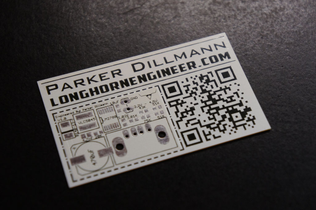
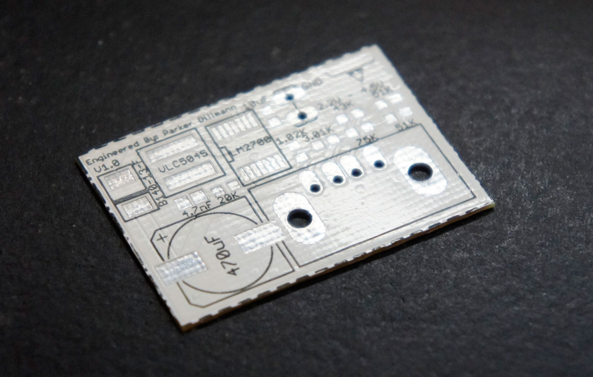
If you received the PCB on a business card you can cut the PCB out around the dotted lines or leave it as is.

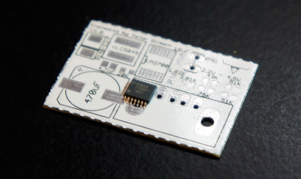
Start by tacking the LM2700 chip down with a soldering iron in a single corner.

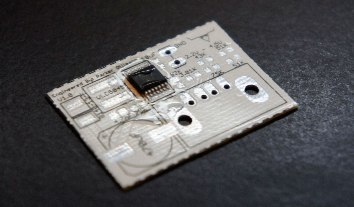
I usually tack down the pin 1 on the chip then apply some flux then finish the chip. After soldering the LM2700 down solder the resistors down.

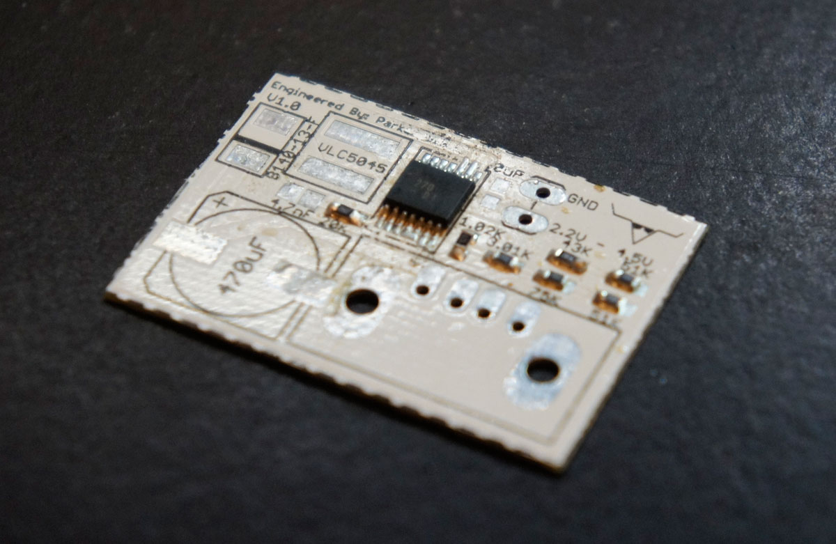
Then the two small SMD capacitors.

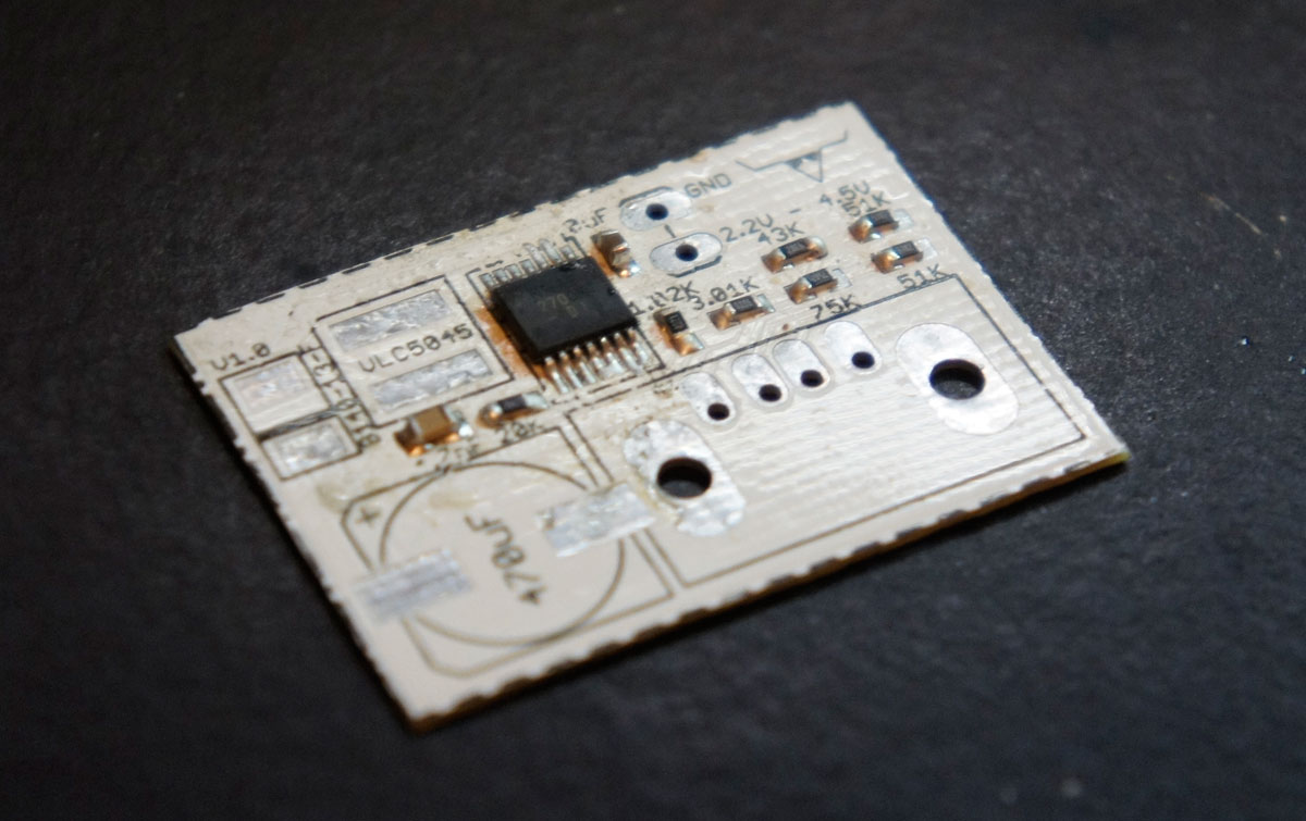
The inductor, diode, and large 470uF capacitor should be soldered next. The inductor is non polarized but care should be taken with the 470uF cap and diode to make sure they are originated correctly.

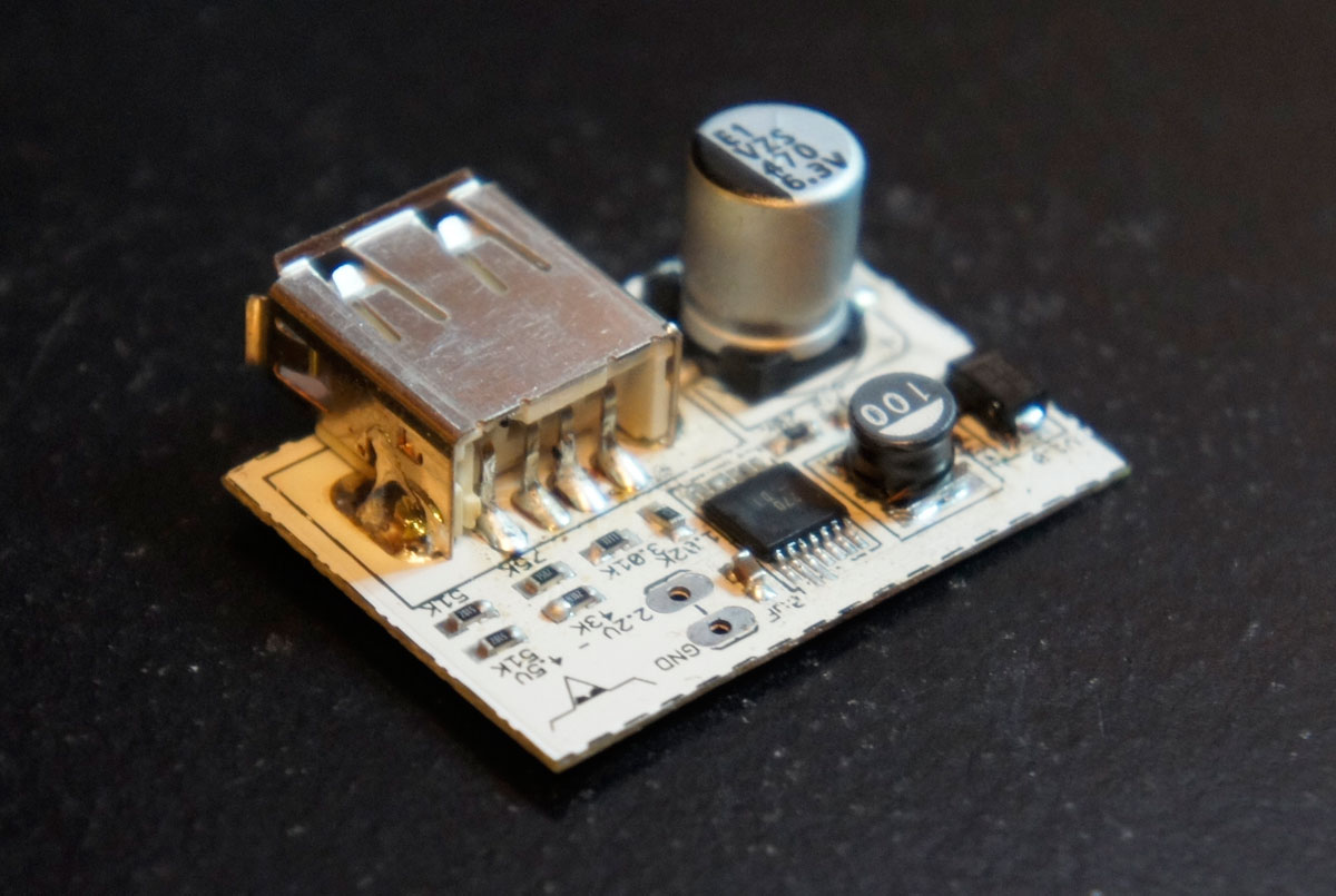
The USB port is the last thing to install. Before connecting your device to charge it use a multimeter and verify that 5V is across the 470uF capacitor terminals.

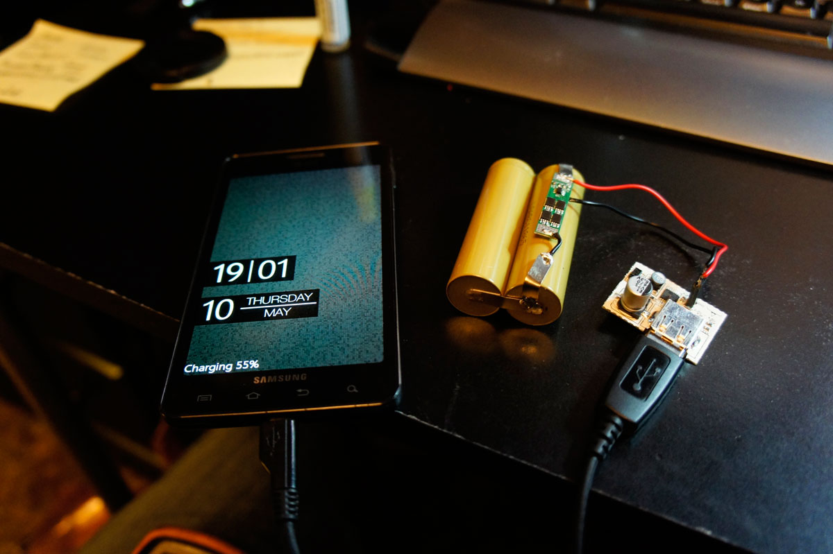
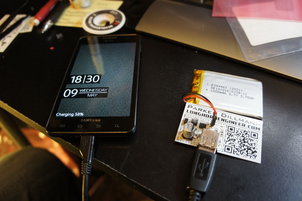
Success! Android phone charging. It is charging at a steady rate of 750mA.

Super Boost Schematic

This design is inspired by the Minty Boost but it fixes some of the issues in that design. The Minty Boost is limited to 600mA due to the LT1302 chip. The Super Boost uses the LM2700 which can push up to 3.6A. This will enable iPhones to charge much more quickly.

Charging more quickly will drain and reduce the life span of AA batteries so lithium batteries are the ideal source.

Tweaking the 128×32 LEDDMD Verilog

There was a few problems with the code for the 128×32 LEDDMD. Every so often there was flickering at random spots on the screen. This was because of the way the display memory was updated. I already fixed it by putting a dummy state at the end of the display memory update. Doing so actually increased the speed that data could be sent to the FPGA. There is no waiting between the Latch pulls.

The last problem is that there is some slight ghosting on the screen. Due to the way the screen updates it looks like the Column data is updating slightly before the rows are updated. Because of this you get a ghost effect on the opposite side of the screen that is up one row.

I think the reason why is because there is a slight delay in the rows caused by the decoders. The current plan of attack is to buffer the Column data a couple cycles before outputting.