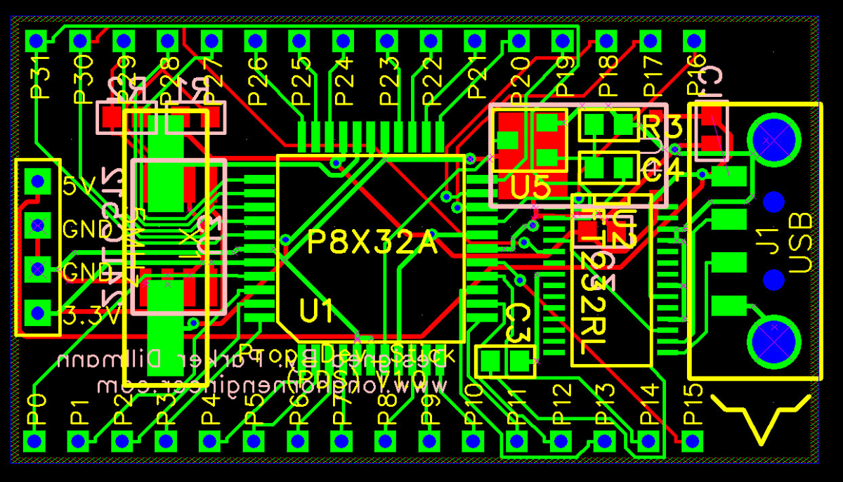
Late night PCB work.

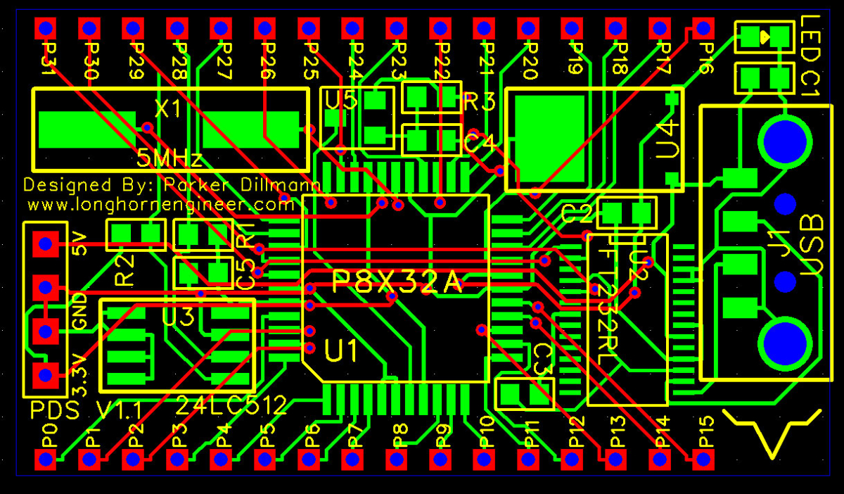
I have had this idea to make a very small development board for the Propeller for a while now. The idea is that you can have it on your keychain or something and just plug the entire unit into a USB port. The port powers the device and there are female headers that allow you to plug other things into it. I might add a ADC just to get some analog signal input.

So I give you /drumroll the Propeller Development Stick or PDS V1.0.

16×96 DMD Code for Reset Vector

While developing the larger 36×128 DMD I ran out of registers and logic elements in the FPGA I was using. I could have switched to a larger FPGA but that would put the final product out of the price range I was aiming for. FPGAs have loads of dedicated ram so I decided to move the display memory from registers to a chunk of block ram. To test to see if the RAM code works I wrote a program for the 16×96 display in RESET_VECTOR. It took a bit of tweaking as I have never used block ram before but I was able to get it working.


module LED_Matrix_16x96
(
clk,row,col,SDRAM_CS,SRAM_CS,LAT,INPUT,SCLK
);

input  wire    clk;
input  wire    LAT;
input  wire    INPUT;
input  wire    SCLK;

output  reg [0:15]  row;
output  reg [95:0]  col;
output  reg [0:0]   SDRAM_CS;
output  reg [0:0]   SRAM_CS;

reg [24:0]  clk_slow;
reg [4:0]  row_cnt;
reg [1535:0]  col_buffer;

reg  [3:0]  read_addr;
reg  [3:0]  write_addr;
reg  [95:0]  disp_mem_data;
reg      disp_mem_wren;
wire  [95:0]  disp_mem_q;

reg [3:0]  sel;

initial
begin
row <= 16'b0000000000000001;
    col <= 16'b0000000000000000;
    SDRAM_CS <= 1'b0;
    SRAM_CS <= 1'b0;
    clk_slow <= 16'b0000000000000000;
    row_cnt <= 5'b00000;
    write_addr <= 4'b0000;
    read_addr <= 4'b0000;
    disp_mem_wren <= 0;
    sel <= 4'b0000;
  end

always @(posedge clk) 
begin
  clk_slow <= clk_slow + 1'b1;

  if(!LAT & row_cnt == 5'b01111)
  begin
  case(sel)
    4'b0000:
    begin
      write_addr <= sel;
      disp_mem_wren <= 1'b1;
      disp_mem_data <= col_buffer[1535:1440];
      sel <= 4'b0001;
    end
    4'b0001:
    begin
      write_addr <= sel;
      disp_mem_wren <= 1'b1;
      disp_mem_data <= col_buffer[1439:1344];
      sel <= 4'b0010;
    end    
    4'b0010:
    begin
      write_addr <= sel;
      disp_mem_wren <= 1'b1;
      disp_mem_data <= col_buffer[1343:1248];
      sel <= 4'b0011;
    end    
    4'b0011:
    begin
      write_addr <= sel;
      disp_mem_wren <= 1'b1;
      disp_mem_data <= col_buffer[1247:1152];
      sel <= 4'b0100;
    end    
    4'b0100:
    begin
      write_addr <= sel;
      disp_mem_wren <= 1'b1;
      disp_mem_data <= col_buffer[1151:1056];
      sel <= 4'b0101;
    end    
    4'b0101:
    begin
      write_addr <= sel;
      disp_mem_wren <= 1'b1;
      disp_mem_data <= col_buffer[1055:960];
      sel <= 4'b0110;
    end
    4'b0110:
    begin
      write_addr <= sel;
      disp_mem_wren <= 1'b1;
      disp_mem_data <= col_buffer[959:864];
      sel <= 4'b0111;
    end
    4'b0111:
    begin
      write_addr <= sel;
      disp_mem_wren <= 1'b1;
      disp_mem_data <= col_buffer[863:768];
      sel <= 4'b1000;
    end
    4'b1000:
    begin
      write_addr <= sel;
      disp_mem_wren <= 1'b1;
      disp_mem_data <= col_buffer[767:672];
      sel <= 4'b1001;
    end
    4'b1001:
    begin
      write_addr <= sel;
      disp_mem_wren <= 1'b1;
      disp_mem_data <= col_buffer[671:576];
      sel <= 4'b1010;
    end    
    4'b1010:
    begin
      write_addr <= sel;
      disp_mem_wren <= 1'b1;
      disp_mem_data <= col_buffer[575:480];
      sel <= 4'b1011;
    end
    4'b1011:
    begin
      write_addr <= sel;
      disp_mem_wren <= 1'b1;
      disp_mem_data <= col_buffer[479:384];
      sel <= 4'b1100;
    end
    4'b1100:
    begin
      write_addr <= sel;
      disp_mem_wren <= 1'b1;
      disp_mem_data <= col_buffer[383:288];
      sel <= 4'b1101;
    end
    4'b1101:
    begin
      write_addr <= sel;
      disp_mem_wren <= 1'b1;
      disp_mem_data <= col_buffer[287:192];
      sel <= 4'b1110;
    end
    4'b1110:
    begin
      write_addr <= sel;
      disp_mem_wren <= 1'b1;
      disp_mem_data <= col_buffer[191:96];
      sel <= 4'b1111;
    end
    4'b1111:
    begin
      write_addr <= sel;
      disp_mem_wren <= 1'b1;
      disp_mem_data <= col_buffer[95:0];
      sel <= 4'b0000;
    end
    default: 
    begin
      sel <= 4'b0000;
      write_addr <= 4'b0000;
      disp_mem_wren <= 1'b0;
    end
  endcase
  end
  else
  begin
    disp_mem_wren <= 1'b0;
    sel <= 4'b0000;
  end
end

always @(posedge clk_slow[10]) 
begin
  if(row_cnt > 5'b01111)
begin
row_cnt <= 5'b00000;
  end
  col <= disp_mem_q;  
  row_cnt <= row_cnt + 1'b1;
  row <= {row[15],row[0:14]};
  read_addr <= read_addr + 1'b1;

end

always @(posedge SCLK)
begin
  if(LAT)
  begin
    col_buffer <= {col_buffer[1534:0],INPUT};
  end
end

display_ram disp_mem_inst (
        .rdaddress (read_addr),
        .wraddress (write_addr),
        .clock  (clk),
        .data   (disp_mem_data),
        .wren   (disp_mem_wren),
        .q      (disp_mem_q)
);

endmodule

MSP-430: Servo and Accel demo Update

Awhile ago I uploaded a demo of the Fraunch Board that used the Accelerometer and outputted it to a set of servos. I made a video demonstrating it but I forgot to upload it.

http://www.youtube.com/watch?v=HttK_tMvNzM

The MSP-EXP430FR5739 board has a built in AXL335 which is a 3-axis accelerometer. It is hard wired to ports P3.0, P3.1, and P3.2. There was no demo code how to get the ADC10 to read those values.

I looked into the sequential sampling that the MSP430 supports which is where ADC10INCHx is set to the last ADC port and will go all the way down to ADC10INCH0 in sequence. This is a problem on the Fraunch Pad as the AXL335 outputs are wired to P3.0 – P3.2 which means when you set ADC10INCHx to ADC10INCH14 (P3.2) it will process more then half the pins as analog inputs!

Solution was to change the ADC10INCHx between sampling so the ADC process became round robin style. Here is the working code to sample all the axises on the Fraunch board. Also included is the “zero” calibration routines.

This code also contains a twin servo routine. The servos are connected to P1.4 and P1.5. When the X-axis moves the servo on P1.4 moves and when the Y-axis moves the servo on P1.5.

Code


main.c
FR_EXP.h

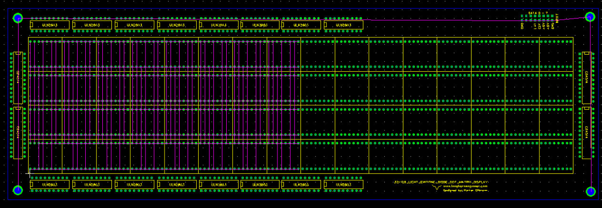
32×128 DMD Rat Lining Halfway Done

Halfway done with the rat lining for the PCB. A rat line is basically a visible line while PCB drawing that indicates net lists. A net list is just a list of all the pins and connections that are connected together. After I rat line I can lay down the traces.

The FPGA sees the display as a 64×64. This is due to I/O limitations. The odd rows are on the left and the even rows are on the right. So row 1 and 2 really make up the physical row 1.

More Verilog Code

Sorry for the massive amount of code recently. To test to see if the RAM code works I wrote a program for the 16×96 display in RESET_VECTOR. If this works then I will order the PCB for the 32×128 DMD. If anyone has any suggestions please feel free to comment. This is the first time I have tried interfacing RAM on an FPGA before.


module LED_Matrix_16x96
(
  clk,row,col,SDRAM_CS,SRAM_CS,LAT,INPUT,SCLK
);

input  wire    clk;
input  wire    LAT;
input  wire    INPUT;
input  wire    SCLK;

output  reg [0:15]  row;
output  reg [95:0]  col;
output  reg [0:0]   SDRAM_CS;
output  reg [0:0]   SRAM_CS;

    reg [24:0]  clk_slow;
    reg [4:0]  row_cnt;
    reg [1535:0]  col_buffer;
    
    reg  [3:0]  read_addr;
    reg  [3:0]  write_addr;
    reg  [95:0]  disp_mem_data;
    reg      disp_mem_wren;
    wire  [95:0]  disp_mem_q;
    
    reg [3:0]  sel;

initial 
  begin
    row <= 16'b0000000000000001;
    col <= 16'b0000000000000000;
    SDRAM_CS <= 1'b0;
    SRAM_CS <= 1'b0;
    clk_slow <= 16'b0000000000000000;
    row_cnt <= 5'b00000;
    write_addr <= 4'b0000;
    read_addr <= 4'b0000;
    disp_mem_wren <= 0;
    sel <= 4'b0000;
  end
  
always @(posedge clk) 
begin
  clk_slow <= clk_slow + 1'b1;
  
  if(!LAT & row_cnt == 5'b01111)
  begin
  case(sel)
    4'b0000:
    begin
      write_addr <= sel;
      disp_mem_wren <= 1'b1;
      disp_mem_data <= col_buffer[1535:1440];
      sel <= 4'b0001;
    end
    4'b0001:
    begin
      write_addr <= sel;
      disp_mem_wren <= 1'b1;
      disp_mem_data <= col_buffer[1439:1344];
      sel <= 4'b0010;
    end    
    4'b0010:
    begin
      write_addr <= sel;
      disp_mem_wren <= 1'b1;
      disp_mem_data <= col_buffer[1343:1248];
      sel <= 4'b0011;
    end    
    4'b0011:
    begin
      write_addr <= sel;
      disp_mem_wren <= 1'b1;
      disp_mem_data <= col_buffer[1247:1152];
      sel <= 4'b0100;
    end    
    4'b0100:
    begin
      write_addr <= sel;
      disp_mem_wren <= 1'b1;
      disp_mem_data <= col_buffer[1151:1056];
      sel <= 4'b0101;
    end    
    4'b0101:
    begin
      write_addr <= sel;
      disp_mem_wren <= 1'b1;
      disp_mem_data <= col_buffer[1055:960];
      sel <= 4'b0110;
    end
    4'b0110:
    begin
      write_addr <= sel;
      disp_mem_wren <= 1'b1;
      disp_mem_data <= col_buffer[959:864];
      sel <= 4'b0111;
    end
    4'b0111:
    begin
      write_addr <= sel;
      disp_mem_wren <= 1'b1;
      disp_mem_data <= col_buffer[863:768];
      sel <= 4'b1000;
    end
    4'b1000:
    begin
      write_addr <= sel;
      disp_mem_wren <= 1'b1;
      disp_mem_data <= col_buffer[767:672];
      sel <= 4'b1001;
    end
    4'b1001:
    begin
      write_addr <= sel;
      disp_mem_wren <= 1'b1;
      disp_mem_data <= col_buffer[671:576];
      sel <= 4'b1010;
    end    
    4'b1010:
    begin
      write_addr <= sel;
      disp_mem_wren <= 1'b1;
      disp_mem_data <= col_buffer[575:480];
      sel <= 4'b1011;
    end
    4'b1011:
    begin
      write_addr <= sel;
      disp_mem_wren <= 1'b1;
      disp_mem_data <= col_buffer[479:384];
      sel <= 4'b1100;
    end
    4'b1100:
    begin
      write_addr <= sel;
      disp_mem_wren <= 1'b1;
      disp_mem_data <= col_buffer[383:288];
      sel <= 4'b1101;
    end
    4'b1101:
    begin
      write_addr <= sel;
      disp_mem_wren <= 1'b1;
      disp_mem_data <= col_buffer[287:192];
      sel <= 4'b1110;
    end
    4'b1110:
    begin
      write_addr <= sel;
      disp_mem_wren <= 1'b1;
      disp_mem_data <= col_buffer[191:96];
      sel <= 4'b1111;
    end
    4'b1111:
    begin
      write_addr <= sel;
      disp_mem_wren <= 1'b1;
      disp_mem_data <= col_buffer[95:0];
      sel <= 4'b0000;
    end
    default: 
    begin
      sel <= 4'b0000;
      write_addr <= 4'b0000;
      disp_mem_wren <= 1'b0;
    end
  endcase
  end
  else
  begin
    disp_mem_wren <= 1'b0;
    sel <= 4'b0000;
  end
end

always @(posedge clk_slow[10]) 
begin
  if(row_cnt > 5'b01111)
  begin
    row_cnt <= 5'b00000;
  end
  col <= disp_mem_q;  
  row_cnt <= row_cnt + 1'b1;
  row <= {row[15],row[0:14]};
  read_addr <= read_addr + 1'b1;
  
end
  
always @(posedge SCLK)
begin
  if(LAT)
  begin
    col_buffer <= {col_buffer[1534:0],INPUT};
  end
end

display_ram disp_mem_inst (
        .rdaddress (read_addr),
        .wraddress (write_addr),
        .clock  (clk),
        .data   (disp_mem_data),
        .wren   (disp_mem_wren),
        .q      (disp_mem_q)
);

endmodule
Updated Code for the 128×32 DMD

The old program took to make Logic elements to fit. Now it uses a 2-port RAM element to replace the huge registers. The protocol for shifting in is a bit different now. Instead of shifting in all the data at once and then Latching the user shifts in the data 64 bits at a time then latches.


module LED_Matrix_32x128
(
clk,e_cnt,row_cnt,col,SDRAM_CS,SRAM_CS,LAT,INPUT,SCLK
);

input  wire  clk;
input  wire  LAT;
input  wire  [7:0]  INPUT;
input  wire  SCLK;

output  reg [63:0]  col;
output  reg [0:0]   SDRAM_CS;
output  reg [0:0]   SRAM_CS;
output  reg [5:0]  row_cnt;
output  reg [4:0]  e_cnt;

reg [24:0]  clk_slow;
reg [63:0]  col_buffer;

    reg  [5:0]  read_addr;
reg  [5:0]  write_addr;
reg  [63:0]  disp_mem_data;
reg      disp_mem_wren;
wire  [63:0]  disp_mem_q;
initial
begin
SDRAM_CS &lt;= 1'b0;
    SRAM_CS &lt;= 1'b0;
    clk_slow &lt;= 16'b0000000000000000;
    row_cnt &lt;= 5'b00000;
    e_cnt &lt;= 4'b1000;
    write_addr &lt;= 5'b00000;
    disp_mem_wren &lt;= 0;
  end

always @(posedge clk) 
begin
  clk_slow &lt;= clk_slow + 1'b1;
end

always @(posedge clk_slow[10]) 
begin
  if(row_cnt &gt; 5'b01111)
begin
row_cnt &lt;= 5'b00000;
    e_cnt &lt;= {e_cnt[2:0],e_cnt[3]};
  end

  col &lt;= disp_mem_q;  
  row_cnt &lt;= row_cnt + 1'b1;
  read_addr &lt;= read_addr + 1'b1;

end

always @(posedge SCLK)
begin
  if(LAT)
  begin
    col_buffer &lt;= {col_buffer[62:0],INPUT[0]};
  end
  else
  begin
    disp_mem_data &lt;= col_buffer;
    disp_mem_wren &lt;= 1;
    disp_mem_wren &lt;= 0;
    write_addr &lt;= write_addr + 1'b1;
  end
end

display_memory disp_mem_inst (
        .rdaddress (read_addr),
        .wraddress (write_addr),
        .clock  (clk),
        .data   (disp_mem_data),
        .wren   (disp_mem_wren),
        .q      (disp_mem_q)
);

endmodule