This is the project that the DE0 Digital IO Wing is for. I will use the IO wing to level shift the signals from the Gameboy’s LCD screen so my DE0 can capture the data. The Gameboy is a 5V device and the DE0 does not have 5V tolerant IO. I am using a SN74LVC8T245PWR 8-bit directional level shifter to do the translation on the IO wing board.
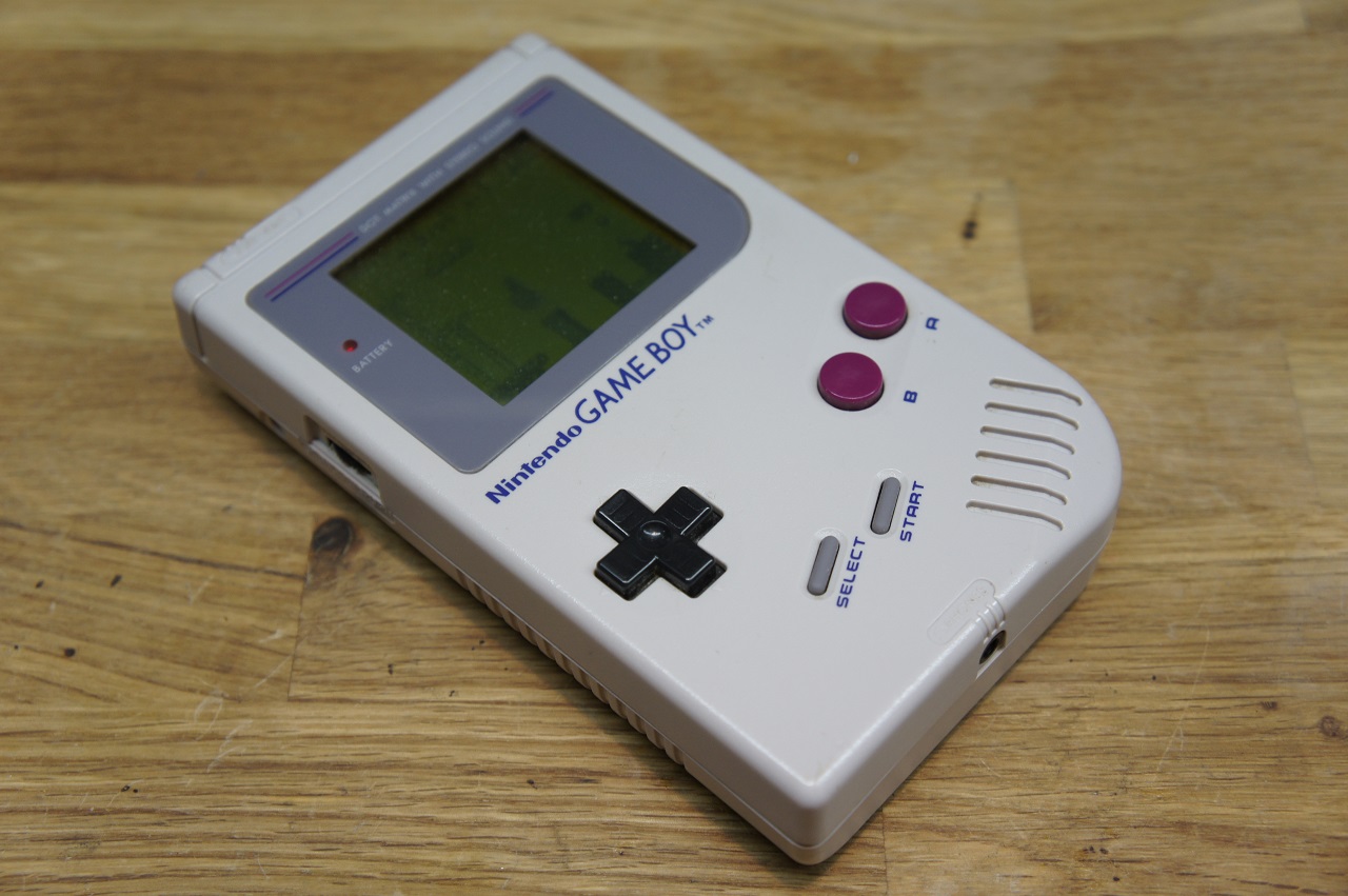
Purchased a Gameboy DMG-01 off eBay for $20. Needed some cleaning but it worked and had the battery cover!
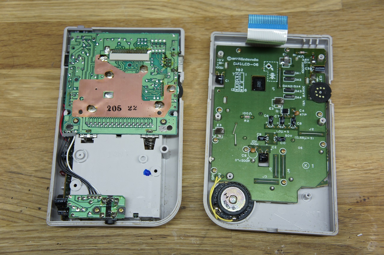
The Gameboy DMG-01 uses triwing screws. Kidna like philips heads but with 3 “wings” instead of 4. Tool can be found on eBay or Amazon.
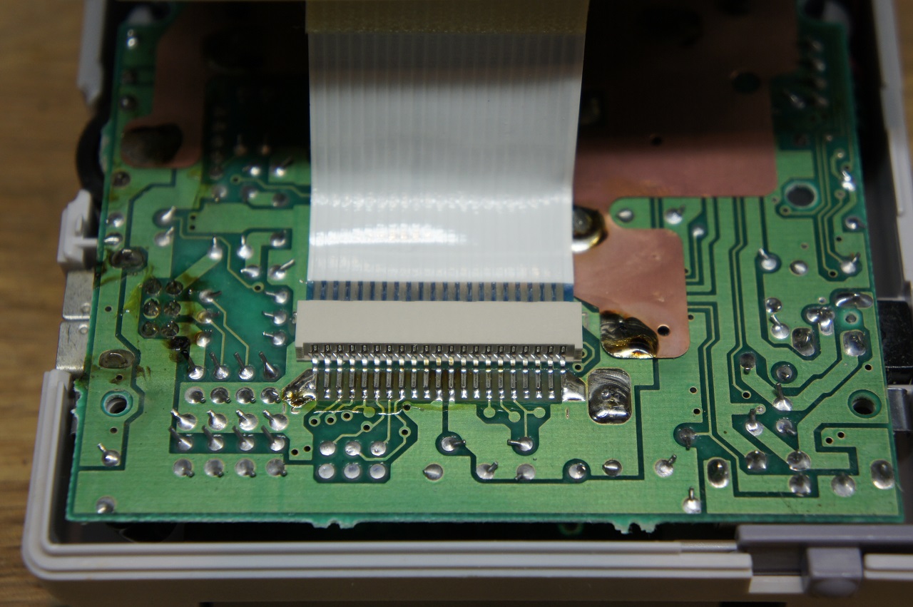
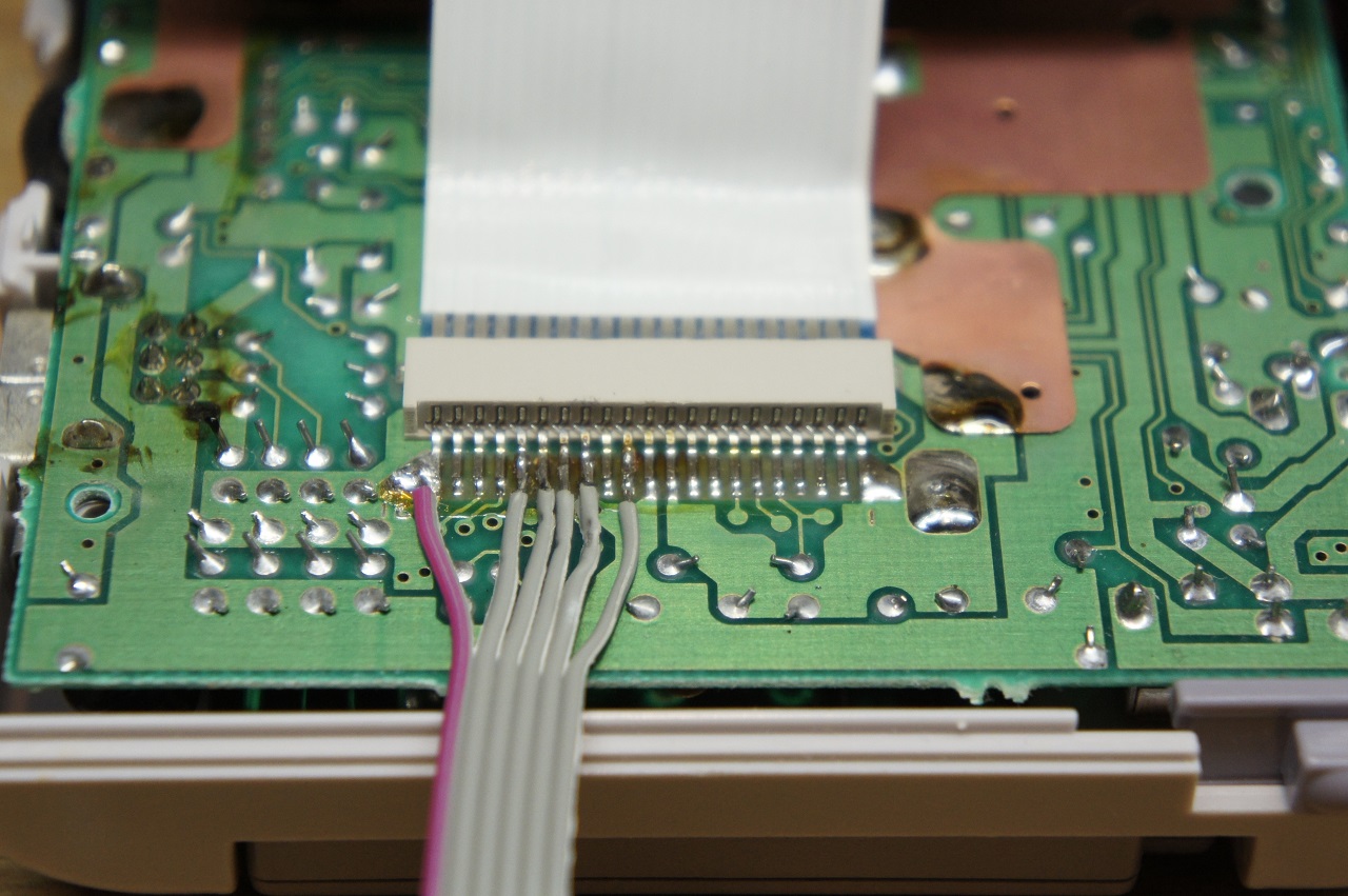
The connector between the front and back of the Gameboy is where I will tap into the signals to sneak a peak. Pinout is the following
Pin 12 – V-Sync
Pin 14 – Pixel Clock
Pin 15 – LCD Data 0
Pin 16 – LCD Data 1
Pin 17 – H-Sync
Pin 21 – Ground
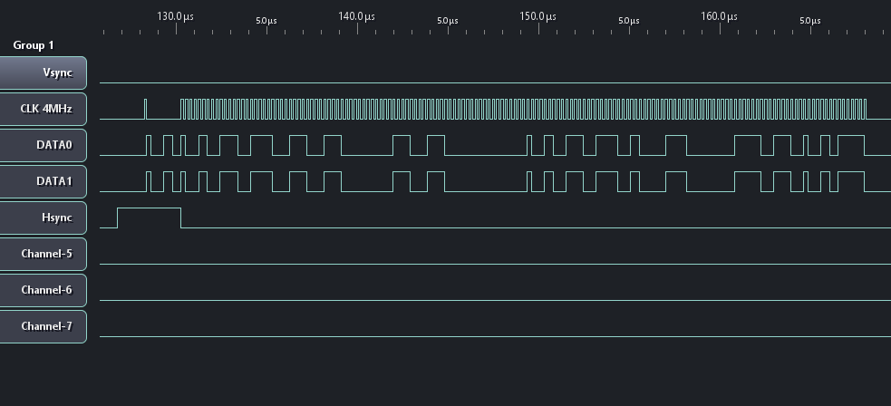
V-Sync should be 60Hz, Pixel Clock 4Mhz, and H-Sync 9.2kHz.
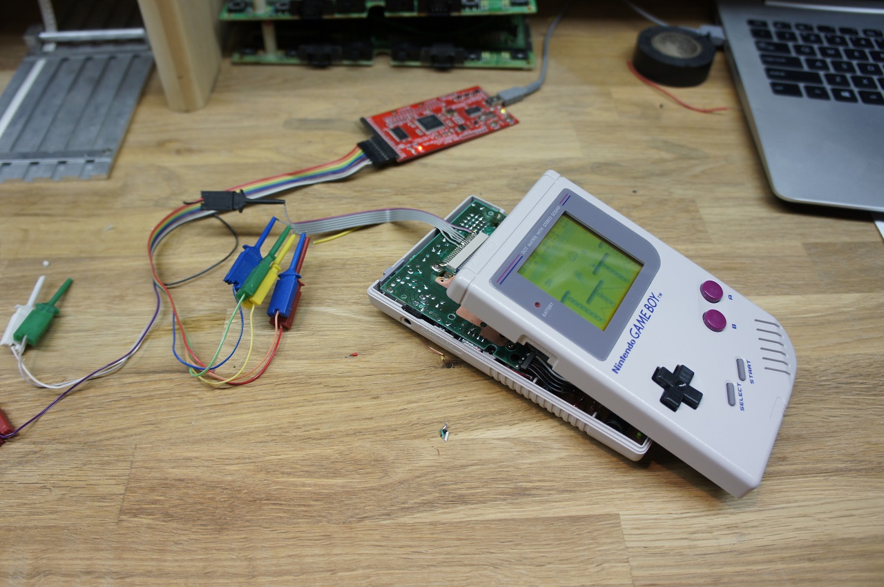
Connected up the Open Bench Logic Sniffer and powered up the Gameboy with a game in it then ran the capture. I had the trigger set to wait for the V-Sync signal.


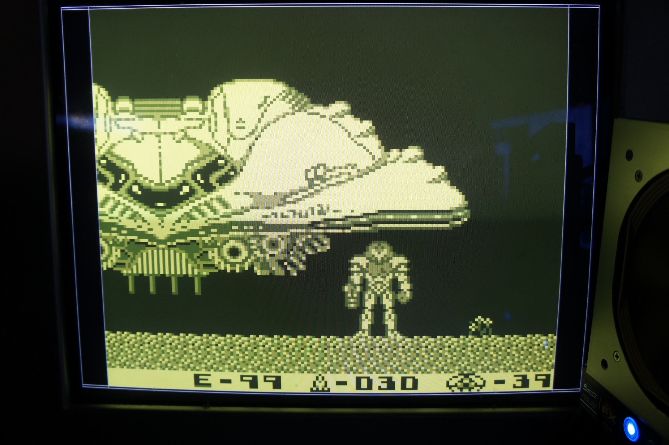
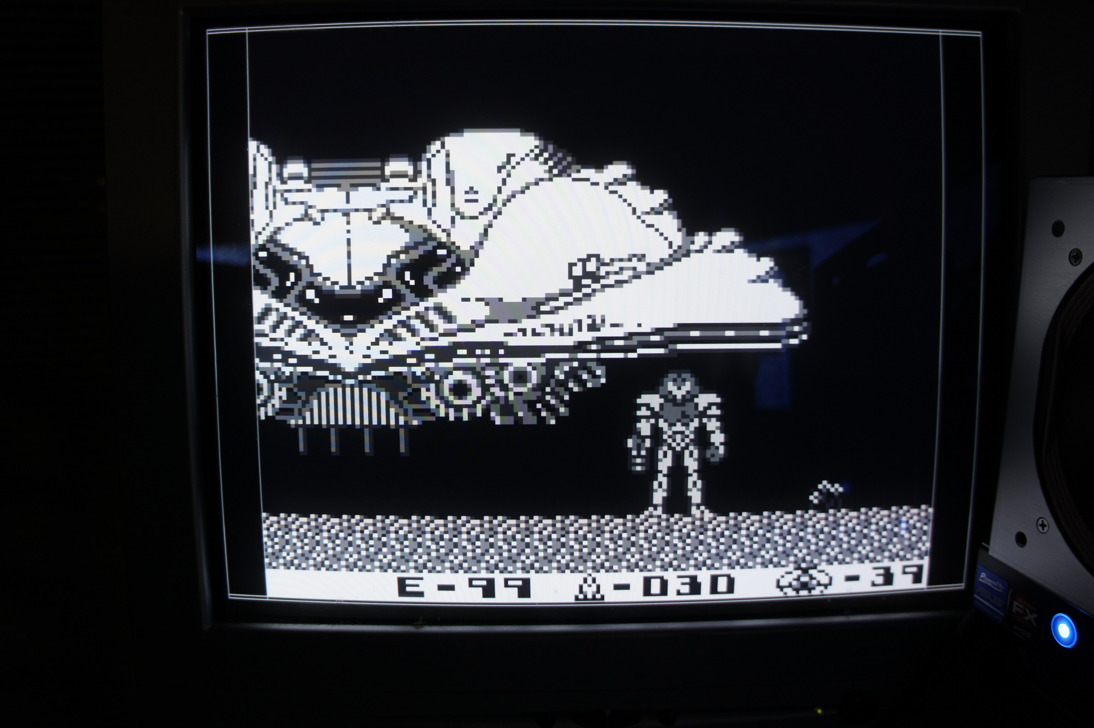
Then using my DE0_VGA_Driver I started writing the code take data from RAM on the FPGA and output it on the VGA monitor. I wrote a bitmap to .mif format (memory initialization file) convertor to display some Gameboy screenshots on the VGA Monitor. Link to that repo is here.
Currently working on getting the SN74LVC8T245PWR level shifters working and I will be able to pull live data from the Gameboy LCD data bus.